Communications Physics ( IF 5.4 ) Pub Date : 2020-03-06 , DOI: 10.1038/s42005-020-0298-2 Shota Kita , Kengo Nozaki , Kenta Takata , Akihiko Shinya , Masaya Notomi
|
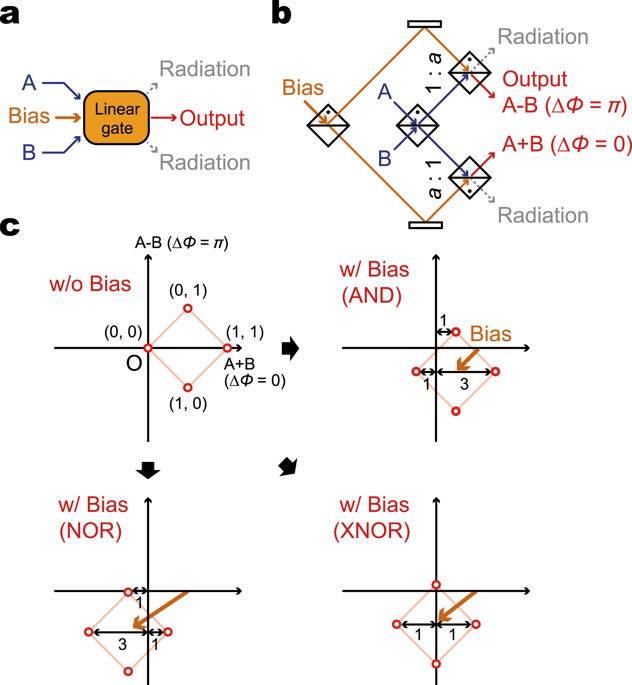
Nonlinear optical gates are usually considered as fundamental building blocks for universal optical computation. However, the performance is severely limited by small optical nonlinearity, thereby bounding their operation speed, consumption energy, and device size. In this paper, we propose and experimentally demonstrate linear optical logic operations with ~3 μm-long Si wire “Ψ” gates consist of 3 × 1 optical combiners including auxiliary bias port, which maximizes the binary contrast of the output in telecom wavelength. We have demonstrated 20 Gbps Boolean “AND” operation with experimentally measured small signal loss (1.6 dB experimentally). A single Ψ gate can perform representative Boolean operations by changing the bias power and relative phases. We have also demonstrated wavelength-independent operation by seven wavelengths, which leads to wavelength-division multiplexed parallel computation. This ultrashort, highly-integrable, low-loss, and energy-efficient optical logic gates pave the way for ultralow latency optical pattern matching, recognition, and conversion.
中文翻译:
用于Si光子平台上的线性光学逻辑的超短低损耗Ψ门
非线性光闸通常被认为是通用光学计算的基本组成部分。然而,由于小的光学非线性严重地限制了性能,从而限制了它们的工作速度,能耗和器件尺寸。在本文中,我们提出并通过实验证明了〜3μm长的Si线“Ψ”门由3×1光学组合器(包括辅助偏置端口)组成的线性光学逻辑操作,该组合器可在电信波长下最大化输出的二进制对比度。我们已经演示了20 Gbps布尔“与”运算,并通过实验测得的小信号损耗(实验为1.6 dB)。单个Ψ门可以通过改变偏置功率和相对相位来执行代表性的布尔运算。我们还通过七个波长展示了与波长无关的操作,这导致波分复用并行计算。这种超短,高度集成,低损耗和高能效的光学逻辑门为超低延迟光学图案匹配,识别和转换铺平了道路。


 京公网安备 11010802027423号