当前位置:
X-MOL 学术
›
ACS Appl. Electron. Mater.
›
论文详情
Our official English website, www.x-mol.net, welcomes your
feedback! (Note: you will need to create a separate account there.)
Low-Temperature Ohmic Contacts to n-ZnSe for all-Electrical Quantum Devices
ACS Applied Electronic Materials ( IF 4.3 ) Pub Date : 2020-03-02 , DOI: 10.1021/acsaelm.9b00824 Johanna Janßen 1, 2 , Felix Hartz 3 , Till Huckemann 3 , Christian Kamphausen 3 , Malte Neul 3 , Lars R. Schreiber 3 , Alexander Pawlis 1
ACS Applied Electronic Materials ( IF 4.3 ) Pub Date : 2020-03-02 , DOI: 10.1021/acsaelm.9b00824 Johanna Janßen 1, 2 , Felix Hartz 3 , Till Huckemann 3 , Christian Kamphausen 3 , Malte Neul 3 , Lars R. Schreiber 3 , Alexander Pawlis 1
Affiliation
|
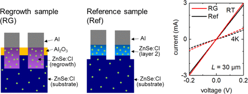
The II/VI semiconductor ZnSe is an ideal host for novel devices for quantum computation and communication as it can be made nuclear-spin free to obtain long electron spin coherence times, exhibits no electron valley-degeneracy, and allows optical access. A prerequisite to electrical quantum devices is low-resistive Ohmic contacts operating at temperatures below 10 K, which have not been achieved in ZnSe yet. Here, we present a comprehensive study on the realization of Ohmic contacts to ZnSe by three different technological approaches, ion implantation of halogen donors, epitaxial doping with in situ contact processing, and finally, a unique ZnSe regrowth technique. The latter allows fabrication of Ohmic contacts with local doping that can be used to connect to a buried conducting channel such as those used in unipolar devices. DC measurements revealed high contact resistivity for Ohmic contacts to ZnSe doped via halogene ion implantation, while in situ aluminum (Al) contacts on epitaxially chlorine-doped ZnSe yield record low contact resistivities in the order of 10–5 Ω cm2 even at cryogenic temperatures. Finally, making use of the regrowth technique, local Ohmic contacts to ZnSe are demonstrated, which still feature low contact resistivities of (1.4 ± 0.4) × 10–3 Ω cm2 at 4 K. These findings pave the way for new electrical devices in the ZnSe material system such as field-effect transistors, electrostatically defined qubits, or quantum repeaters operating at cryogenic temperatures.
中文翻译:

全电子量子器件的与n -ZnSe的低温欧姆接触
II / VI半导体ZnSe是用于量子计算和通信的新型设备的理想主机,因为它可以被制成无核自旋的,以获得长的电子自旋相干时间,没有电子波谷简并可以进行光学访问。电量子器件的先决条件是在低于10 K的温度下运行的低电阻欧姆接触,而ZnSe尚未实现。在这里,我们对通过三种不同的技术方法实现与ZnSe的欧姆接触进行全面研究,包括卤素供体的离子注入,通过原位接触处理进行外延掺杂以及最后一种独特的ZnSe再生技术。后者允许制造具有局部掺杂的欧姆接触,该欧姆接触可用于连接至掩埋的导电沟道,例如单极器件中使用的沟道。-5 Ω厘米2,甚至在低温下。最后,利用所述再生长技术的,局部欧姆接触到的ZnSe被证明的,仍设有的(1.4±0.4)×10低的接触电阻率-3 Ω厘米2,在4 K.这些发现铺路在新的电气装置ZnSe材料系统,例如场效应晶体管,静电定义的量子位或在低温下工作的量子中继器。
更新日期:2020-03-02
中文翻译:
全电子量子器件的与n -ZnSe的低温欧姆接触
II / VI半导体ZnSe是用于量子计算和通信的新型设备的理想主机,因为它可以被制成无核自旋的,以获得长的电子自旋相干时间,没有电子波谷简并可以进行光学访问。电量子器件的先决条件是在低于10 K的温度下运行的低电阻欧姆接触,而ZnSe尚未实现。在这里,我们对通过三种不同的技术方法实现与ZnSe的欧姆接触进行全面研究,包括卤素供体的离子注入,通过原位接触处理进行外延掺杂以及最后一种独特的ZnSe再生技术。后者允许制造具有局部掺杂的欧姆接触,该欧姆接触可用于连接至掩埋的导电沟道,例如单极器件中使用的沟道。-5 Ω厘米2,甚至在低温下。最后,利用所述再生长技术的,局部欧姆接触到的ZnSe被证明的,仍设有的(1.4±0.4)×10低的接触电阻率-3 Ω厘米2,在4 K.这些发现铺路在新的电气装置ZnSe材料系统,例如场效应晶体管,静电定义的量子位或在低温下工作的量子中继器。


 京公网安备 11010802027423号