当前位置:
X-MOL 学术
›
Photonics Res.
›
论文详情
Our official English website, www.x-mol.net, welcomes your feedback! (Note: you will need to create a separate account there.)
In-depth investigation and applications of novel silicon photonics microstructures supporting optical vorticity and waveguiding for ultra narrowband near-infrared perfect absorption
Photonics Research ( IF 7.6 ) Pub Date : 2020-02-28 , DOI: 10.1364/prj.375802 Roy Avrahamy , Moshe Zohar , Mark Auslender , Benny Milgrom , Shlomo Hava , Rafi Shikler
Photonics Research ( IF 7.6 ) Pub Date : 2020-02-28 , DOI: 10.1364/prj.375802 Roy Avrahamy , Moshe Zohar , Mark Auslender , Benny Milgrom , Shlomo Hava , Rafi Shikler
|
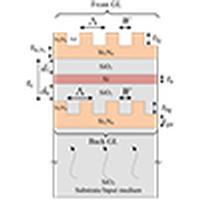
We propose a novel concept of designing silicon photonics metamaterials for perfect near-infrared light absorption. The study’s emphasis is an in-depth investigation of various physical mechanisms behind the ∼100% ultra-narrowband record peak absorptance of the designed structures, comprising an ultrathin silicon absorber. The electromagnetic power transport, described by the Poynting vector, is innovatively explored, which shows combined vortex and crossed-junction two-dimensional waveguide-like flows as outcomes of optical field singularities. These flows, though peculiar for each of the designed structures, turn out to be key factors of the perfect resonant optical absorption. The electromagnetic fields show tight two-dimensional confinement: a sharp vertical confinement of the resonant-cavity type combined with a lateral metasurface supported confinement. The silicon-absorbing layer and its oxide environment are confined between two subwavelength metasurfaces such that the entire design is well compatible with silicon-on-insulator microelectronics. The design concept and its outcomes meet the extensive challenges of ultrathin absorbers for minimum noise and an ultra-narrowband absorptance spectrum, while maintaining an overall very thin structure for planar integration. With these materials and such objectives, the proposed designs seem essential, as standard approaches fail, mainly due to a very low silicon absorption coefficient over the near-infrared range. Tolerance tests for fabrication errors show fair tolerability while maintaining a high absorptance peak, along with a controllable deviation off the central-design wavelength. Various applications are suggested and analyzed, which include but are not limited to: efficient photodetectors for focal plane array and on-chip integrated silicon photonics, high-precision spectroscopic chemical and angular-position sensing, and wavelength-division multiplexing.
中文翻译:

支持光学涡度和波导的新型硅光子微结构用于超窄带近红外完美吸收的深入研究和应用
我们提出了一种设计硅光子超材料的新概念,以实现完美的近红外光吸收。该研究的重点是深入研究设计结构的~100% 超窄带记录峰值吸收率背后的各种物理机制,包括超薄硅吸收体。创新性地探索了由坡印廷矢量描述的电磁功率传输,它显示了作为光场奇点结果的组合涡流和交叉结二维波导状流动。这些流动虽然对于每个设计的结构来说都是独特的,但结果却是完美共振光吸收的关键因素。电磁场显示出严格的二维限制:共振腔类型的尖锐垂直限制与横向超表面支持的限制相结合。硅吸收层及其氧化物环境被限制在两个亚波长超表面之间,因此整个设计与绝缘体上硅微电子学很好地兼容。设计理念及其成果满足了超薄吸收器的广泛挑战,以实现最小噪声和超窄带吸收光谱,同时保持整体非常薄的平面集成结构。有了这些材料和这样的目标,所提出的设计似乎是必不可少的,因为标准方法失败了,主要是由于近红外范围内的硅吸收系数非常低。制造错误的容忍度测试显示出良好的容忍度,同时保持高吸收率峰值,以及偏离中心设计波长的可控偏差。建议和分析了各种应用,包括但不限于:用于焦平面阵列和片上集成硅光子学的高效光电探测器、高精度光谱化学和角位置传感以及波分复用。
更新日期:2020-02-28
中文翻译:
支持光学涡度和波导的新型硅光子微结构用于超窄带近红外完美吸收的深入研究和应用
我们提出了一种设计硅光子超材料的新概念,以实现完美的近红外光吸收。该研究的重点是深入研究设计结构的~100% 超窄带记录峰值吸收率背后的各种物理机制,包括超薄硅吸收体。创新性地探索了由坡印廷矢量描述的电磁功率传输,它显示了作为光场奇点结果的组合涡流和交叉结二维波导状流动。这些流动虽然对于每个设计的结构来说都是独特的,但结果却是完美共振光吸收的关键因素。电磁场显示出严格的二维限制:共振腔类型的尖锐垂直限制与横向超表面支持的限制相结合。硅吸收层及其氧化物环境被限制在两个亚波长超表面之间,因此整个设计与绝缘体上硅微电子学很好地兼容。设计理念及其成果满足了超薄吸收器的广泛挑战,以实现最小噪声和超窄带吸收光谱,同时保持整体非常薄的平面集成结构。有了这些材料和这样的目标,所提出的设计似乎是必不可少的,因为标准方法失败了,主要是由于近红外范围内的硅吸收系数非常低。制造错误的容忍度测试显示出良好的容忍度,同时保持高吸收率峰值,以及偏离中心设计波长的可控偏差。建议和分析了各种应用,包括但不限于:用于焦平面阵列和片上集成硅光子学的高效光电探测器、高精度光谱化学和角位置传感以及波分复用。


 京公网安备 11010802027423号