当前位置:
X-MOL 学术
›
ACS Appl. Electron. Mater.
›
论文详情
Our official English website, www.x-mol.net, welcomes your
feedback! (Note: you will need to create a separate account there.)
Enhanced Photoresponse of WS2 Photodetectors through Interfacial Defect Engineering Using a TiO2 Interlayer
ACS Applied Electronic Materials ( IF 4.3 ) Pub Date : 2020-02-26 , DOI: 10.1021/acsaelm.0c00011 Yusin Pak 1 , Woojin Park 2 , Naresh Alaal 1 , Yogeenth Kumaresan 3 , S. Assa Aravindh 4 , Somak Mitra 1 , Bin Xin 1 , Jung-Wook Min 2 , Hyeonghun Kim 3 , Namsoo Lim 3 , Byungjin Cho 5 , Gun-Young Jung 3 , Muhammad M. Hussain 2 , Iman S. Roqan 1
ACS Applied Electronic Materials ( IF 4.3 ) Pub Date : 2020-02-26 , DOI: 10.1021/acsaelm.0c00011 Yusin Pak 1 , Woojin Park 2 , Naresh Alaal 1 , Yogeenth Kumaresan 3 , S. Assa Aravindh 4 , Somak Mitra 1 , Bin Xin 1 , Jung-Wook Min 2 , Hyeonghun Kim 3 , Namsoo Lim 3 , Byungjin Cho 5 , Gun-Young Jung 3 , Muhammad M. Hussain 2 , Iman S. Roqan 1
Affiliation
|
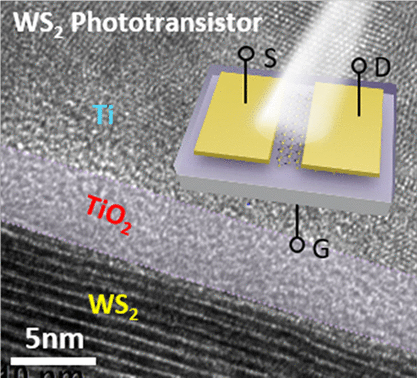
To develop a stable and reliable two-dimensional (2D) tungsten disulfide (WS2)-based photodetector (PD), it is essential to address the issue of interfacial defects that are unavoidably formed at the interface between WS2 and metal contact as such defects can markedly deteriorate photoresponse characteristics. In this work, this drawback is mitigated by adopting a facile technique for passivating a WS2 surface with an ultrathin TiO2 film. The TiO2 interlayer is deposited on the 2D WS2 surface via 20 cycles of atomic layer deposition prior to proceeding with photolithography and contact metal deposition. Advanced characterizations reveal that TiO2/WS2 PDs exhibit enhanced photoresponse compared to bare WS2. Much higher photoresponsivity (∼10 times higher at 1 mW/cm2) and faster recovery (∼124 times faster at 0.1 V) are obtained from TiO2/WS2 PDs relative to bare WS2 PDs. The mechanism underlying the enhanced PD performance is demonstrated. The computational density functional theory using the Heyd–Scuseria–Ernzerhof approach demonstrates the significant role of the TiO2/WS2 interface in facilitating the charge transfer and improving the PD performance compared to the bare WS2 device. This approach paves the way for developing reliable and high-performance 2D WS2-based optoelectronic devices.
中文翻译:

通过使用TiO 2中间层的界面缺陷工程增强了WS 2光电探测器的光响应
为了开发稳定可靠的二维(2D)二硫化钨(WS 2)基光电检测器(PD),必须解决不可避免地在WS 2和金属触点之间的界面上形成的界面缺陷的问题。缺陷会显着降低光响应特性。在这项工作中,通过采用简便的技术以超薄的TiO 2膜钝化WS 2表面来减轻这一缺陷。在进行光刻和接触金属沉积之前,通过20个原子层沉积循环将TiO 2中间层沉积在2D WS 2表面上。先进的表征表明TiO 2 / WS与裸露的WS 2相比,2个PD表现出增强的光响应。相对于裸露的WS 2 PD ,TiO 2 / WS 2 PDs具有更高的光响应性(在1 mW / cm 2时约10倍高)和更快的恢复(在0.1 V时约124倍)恢复。演示了增强的PD性能的机制。使用Heyd–Scuseria–Ernzerhof方法的计算密度泛函理论证明,与裸露WS 2装置相比,TiO 2 / WS 2界面在促进电荷转移和改善PD性能方面发挥了重要作用。这种方法为开发可靠的高性能2D WS铺平了道路基于2的光电设备。
更新日期:2020-02-26
中文翻译:
通过使用TiO 2中间层的界面缺陷工程增强了WS 2光电探测器的光响应
为了开发稳定可靠的二维(2D)二硫化钨(WS 2)基光电检测器(PD),必须解决不可避免地在WS 2和金属触点之间的界面上形成的界面缺陷的问题。缺陷会显着降低光响应特性。在这项工作中,通过采用简便的技术以超薄的TiO 2膜钝化WS 2表面来减轻这一缺陷。在进行光刻和接触金属沉积之前,通过20个原子层沉积循环将TiO 2中间层沉积在2D WS 2表面上。先进的表征表明TiO 2 / WS与裸露的WS 2相比,2个PD表现出增强的光响应。相对于裸露的WS 2 PD ,TiO 2 / WS 2 PDs具有更高的光响应性(在1 mW / cm 2时约10倍高)和更快的恢复(在0.1 V时约124倍)恢复。演示了增强的PD性能的机制。使用Heyd–Scuseria–Ernzerhof方法的计算密度泛函理论证明,与裸露WS 2装置相比,TiO 2 / WS 2界面在促进电荷转移和改善PD性能方面发挥了重要作用。这种方法为开发可靠的高性能2D WS铺平了道路基于2的光电设备。


 京公网安备 11010802027423号