当前位置:
X-MOL 学术
›
ACS Appl. Electron. Mater.
›
论文详情
Our official English website, www.x-mol.net, welcomes your
feedback! (Note: you will need to create a separate account there.)
High-Speed Complementary Integrated Circuit with a Stacked Structure Using Fine Electrodes Formed by Reverse Offset Printing
ACS Applied Electronic Materials ( IF 4.3 ) Pub Date : 2020-02-20 , DOI: 10.1021/acsaelm.9b00829 Yasunori Takeda 1 , Tomohito Sekine 1 , Yi-Fei Wang 1 , Tomoko Okamoto 2 , Hiroyuki Matsui 1 , Daisuke Kumaki 1 , Shizuo Tokito 1
ACS Applied Electronic Materials ( IF 4.3 ) Pub Date : 2020-02-20 , DOI: 10.1021/acsaelm.9b00829 Yasunori Takeda 1 , Tomohito Sekine 1 , Yi-Fei Wang 1 , Tomoko Okamoto 2 , Hiroyuki Matsui 1 , Daisuke Kumaki 1 , Shizuo Tokito 1
Affiliation
|
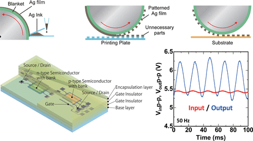
A reverse offset-printed stacked-structure complementary ring oscillator and operational amplifier (OPA) circuits were constructed on a large-area substrate. Uniform and fine electrodes were fabricated using reverse offset printing with a width of 30 μm and a channel length of 10 μm. Compared to silver nanoparticle electrodes constructed using inkjet printing, a narrow line with a width of 1/5 or less could be formed. All components except the insulating film were formed using a solution process with the printing method. The complementary integrated circuit had a stacked structure, wherein a p-type organic thin-film transistor (OTFT) was stacked on an n-type OTFT with a common gate electrode layer. Because the source and drain electrode layers of the n- and p-type OTFTs were separated, different self-assembled monolayers could be treated using a simple method. The complementary ring oscillator circuit oscillated at a frequency of 2 kHz (12.5 V, five stages) and operated at 1.25 V (96 Hz, nine stages). The fabricated OPA circuit had an output/input voltage ratio of 20. Additionally, it operated over 40 times faster than a similar circuit formed by inkjet printing. Fine electrodes formed by reverse offset printing are useful for improving the performance and miniaturization of printed organic integrated circuits.
中文翻译:

使用反向胶版印刷形成的细电极的堆叠结构高速互补集成电路
在大面积基板上构造了反向胶版印刷的堆叠结构互补环形振荡器和运算放大器(OPA)电路。使用反向胶版印刷制造宽度为30μm,通道长度为10μm的均匀电极和精细电极。与使用喷墨印刷构造的银纳米颗粒电极相比,可以形成宽度为1/5或更小的窄线。除了绝缘膜以外的所有部件都是通过印刷法的固溶处理而形成的。互补集成电路具有堆叠结构,其中将p型有机薄膜晶体管(OTFT)堆叠在具有公共栅电极层的n型OTFT上。由于n型和p型OTFT的源电极层和漏电极层是分开的,可以使用一种简单的方法来处理不同的自组装单层膜。互补环形振荡器电路以2 kHz(12.5 V,五级)的频率振荡,并以1.25 V(96 Hz,九级)的频率工作。制成的OPA电路的输出/输入电压比为20。此外,它的运行速度比通过喷墨打印形成的类似电路快40倍以上。通过反向胶版印刷形成的精细电极可用于改善印刷有机集成电路的性能和小型化。
更新日期:2020-02-20
中文翻译:
使用反向胶版印刷形成的细电极的堆叠结构高速互补集成电路
在大面积基板上构造了反向胶版印刷的堆叠结构互补环形振荡器和运算放大器(OPA)电路。使用反向胶版印刷制造宽度为30μm,通道长度为10μm的均匀电极和精细电极。与使用喷墨印刷构造的银纳米颗粒电极相比,可以形成宽度为1/5或更小的窄线。除了绝缘膜以外的所有部件都是通过印刷法的固溶处理而形成的。互补集成电路具有堆叠结构,其中将p型有机薄膜晶体管(OTFT)堆叠在具有公共栅电极层的n型OTFT上。由于n型和p型OTFT的源电极层和漏电极层是分开的,可以使用一种简单的方法来处理不同的自组装单层膜。互补环形振荡器电路以2 kHz(12.5 V,五级)的频率振荡,并以1.25 V(96 Hz,九级)的频率工作。制成的OPA电路的输出/输入电压比为20。此外,它的运行速度比通过喷墨打印形成的类似电路快40倍以上。通过反向胶版印刷形成的精细电极可用于改善印刷有机集成电路的性能和小型化。


 京公网安备 11010802027423号