当前位置:
X-MOL 学术
›
Prog. Photovoltaics
›
论文详情
Our official English website, www.x-mol.net, welcomes your
feedback! (Note: you will need to create a separate account there.)
Doped hydrogenated nanocrystalline silicon oxide layers for high‐efficiency c‐Si heterojunction solar cells
Progress in Photovoltaics ( IF 8.0 ) Pub Date : 2020-02-18 , DOI: 10.1002/pip.3256 Yifeng Zhao 1 , Luana Mazzarella 1 , Paul Procel 1 , Can Han 1, 2, 3 , Guangtao Yang 1 , Arthur Weeber 1, 4 , Miro Zeman 1 , Olindo Isabella 1
Progress in Photovoltaics ( IF 8.0 ) Pub Date : 2020-02-18 , DOI: 10.1002/pip.3256 Yifeng Zhao 1 , Luana Mazzarella 1 , Paul Procel 1 , Can Han 1, 2, 3 , Guangtao Yang 1 , Arthur Weeber 1, 4 , Miro Zeman 1 , Olindo Isabella 1
Affiliation
|
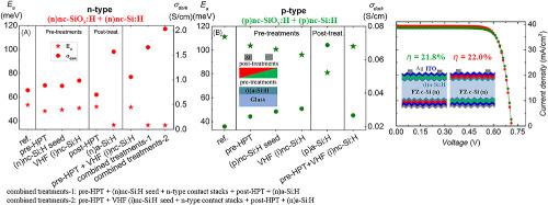
Hydrogenated nanocrystalline silicon oxide (nc‐SiOx:H) layers exhibit promising optoelectrical properties for carrier‐selective‐contacts in silicon heterojunction (SHJ) solar cells. However, achieving high conductivity while preserving crystalline silicon (c‐Si) passivation quality is technologically challenging for growing thin layers (less than 20 nm) on the intrinsic hydrogenated amorphous silicon ((i)a‐Si:H) layer. Here, we present an evaluation of different strategies to improve optoelectrical parameters of SHJ contact stacks founded on highly transparent nc‐SiOx:H layers. Using plasma‐enhanced chemical vapor deposition, we firstly investigate the evolution of optoelectrical parameters by varying the main deposition conditions to achieve layers with refractive index below 2.2 and dark conductivity above 1.00 S/cm. Afterwards, we assess the electrical properties with the application of different surface treatments before and after doped layer deposition. Noticeably, we drastically improve the dark conductivity from 0.79 to 2.03 S/cm and 0.02 to 0.07 S/cm for n‐ and p‐contact, respectively. We observe that interface treatments after (i)a‐Si:H deposition not only induce prompt nucleation of nanocrystals but also improve c‐Si passivation quality. Accordingly, we demonstrate fill factor improvement of 13.5%abs from 65.6% to 79.1% in front/back‐contacted solar cells. We achieve conversion efficiency of 21.8% and 22.0% for front and rear junction configurations, respectively. The optical effectiveness of contact stacks based on nc‐SiOx:H is demonstrated by averagely 1.5 mA/cm2 higher short‐circuit current density thus nearly 1%abs higher cell efficiency as compared with the (n)a‐Si:H.
中文翻译:

用于高效c-Si异质结太阳能电池的掺杂氢化纳米晶氧化硅层
氢化纳米晶氧化硅(nc-SiO x:H)层在硅异质结(SHJ)太阳能电池中表现出有希望的载流子选择接触光电性能。但是,在保持本征氢化非晶硅((i)a-Si:H)层上生长薄层(小于20 nm)的同时,在保持晶体硅(c-Si)钝化质量的同时实现高电导率在技术上具有挑战性。在这里,我们对提高基于高透明nc-SiO x的SHJ接触堆的光电参数的不同策略进行了评估。:H层。我们使用等离子增强化学气相沉积技术,首先通过改变主要沉积条件来研究光电参数的演变,以实现折射率低于2.2且暗电导率高于1.00 S / cm的层。之后,我们在掺杂层沉积之前和之后通过应用不同的表面处理来评估电性能。值得注意的是,对于n-接触和p-接触,我们将暗电导率分别从0.79 S / cm和2.03 S / cm大大提高了。我们观察到(i)a-Si:H沉积后的界面处理不仅可以诱导纳米晶迅速成核,而且可以提高c-Si钝化质量。因此,我们证明填充因子提高了13.5%abs正面/背面接触式太阳能电池从65.6%降至79.1%。对于前结和后结配置,我们分别实现了21.8%和22.0%的转换效率。基于NC-的SiO接触叠层的光学效果X:H是由平均1.5毫安/厘米证明2更高的短路电流密度从而近1%腹肌H:与第(n)相比较高的电池效率的a-Si。
更新日期:2020-02-18
中文翻译:
用于高效c-Si异质结太阳能电池的掺杂氢化纳米晶氧化硅层
氢化纳米晶氧化硅(nc-SiO x:H)层在硅异质结(SHJ)太阳能电池中表现出有希望的载流子选择接触光电性能。但是,在保持本征氢化非晶硅((i)a-Si:H)层上生长薄层(小于20 nm)的同时,在保持晶体硅(c-Si)钝化质量的同时实现高电导率在技术上具有挑战性。在这里,我们对提高基于高透明nc-SiO x的SHJ接触堆的光电参数的不同策略进行了评估。:H层。我们使用等离子增强化学气相沉积技术,首先通过改变主要沉积条件来研究光电参数的演变,以实现折射率低于2.2且暗电导率高于1.00 S / cm的层。之后,我们在掺杂层沉积之前和之后通过应用不同的表面处理来评估电性能。值得注意的是,对于n-接触和p-接触,我们将暗电导率分别从0.79 S / cm和2.03 S / cm大大提高了。我们观察到(i)a-Si:H沉积后的界面处理不仅可以诱导纳米晶迅速成核,而且可以提高c-Si钝化质量。因此,我们证明填充因子提高了13.5%abs正面/背面接触式太阳能电池从65.6%降至79.1%。对于前结和后结配置,我们分别实现了21.8%和22.0%的转换效率。基于NC-的SiO接触叠层的光学效果X:H是由平均1.5毫安/厘米证明2更高的短路电流密度从而近1%腹肌H:与第(n)相比较高的电池效率的a-Si。


 京公网安备 11010802027423号