当前位置:
X-MOL 学术
›
ACS Photonics
›
论文详情
Our official English website, www.x-mol.net, welcomes your
feedback! (Note: you will need to create a separate account there.)
Inverse-Designed Photonics for Semiconductor Foundries
ACS Photonics ( IF 6.5 ) Pub Date : 2020-02-20 , DOI: 10.1021/acsphotonics.9b01540 Alexander Y. Piggott 1 , Eric Y. Ma 1, 2 , Logan Su 1 , Geun Ho Ahn 1 , Neil V. Sapra 1 , Dries Vercruysse 1 , Andrew M. Netherton 3 , Akhilesh S. P. Khope 3 , John E. Bowers 3 , Jelena Vučković 1
ACS Photonics ( IF 6.5 ) Pub Date : 2020-02-20 , DOI: 10.1021/acsphotonics.9b01540 Alexander Y. Piggott 1 , Eric Y. Ma 1, 2 , Logan Su 1 , Geun Ho Ahn 1 , Neil V. Sapra 1 , Dries Vercruysse 1 , Andrew M. Netherton 3 , Akhilesh S. P. Khope 3 , John E. Bowers 3 , Jelena Vučković 1
Affiliation
|
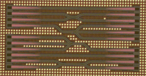
Silicon photonics is becoming a leading technology in photonics, displacing traditional fiber optic transceivers and enabling new applications. Further improving the density and performance of silicon photonics, however, has been challenging due to the large size and limited performance of traditional semianalytically designed components. Automated optimization of photonic devices using inverse design is a promising path forward but has, until now, faced difficulties in producing designs that can be fabricated reliably at scale. Here we experimentally demonstrate four inverse-designed devices made successfully in a commercial silicon photonics foundry: a spatial mode multiplexer, wavelength demultiplexer, 50–50 directional coupler, and 3-way power splitter. These devices are efficient, robust to fabrication variability, and compact, with footprints only a few micrometers across. They pave the way forward for the widespread practical use of inverse design.
中文翻译:

半导体代工厂的反设计光子学
硅光子学正成为光子学中的领先技术,取代了传统的光纤收发器并实现了新的应用。然而,由于传统的半解析设计组件的大尺寸和有限的性能,进一步提高硅光子学的密度和性能一直是具有挑战性的。使用逆向设计对光子器件进行自动优化是一个有前途的发展方向,但是直到现在,在生产可以可靠地大规模制造的设计方面仍然面临着困难。在这里,我们通过实验演示了在商业硅光子铸造厂成功制造的四个反向设计的设备:空间模式多路复用器,波长解复用器,50–50定向耦合器和三路功率分配器。这些设备效率高,制造可变性强,结构紧凑,占地面积只有几微米。它们为逆设计的广泛实际应用铺平了道路。
更新日期:2020-02-20
中文翻译:
半导体代工厂的反设计光子学
硅光子学正成为光子学中的领先技术,取代了传统的光纤收发器并实现了新的应用。然而,由于传统的半解析设计组件的大尺寸和有限的性能,进一步提高硅光子学的密度和性能一直是具有挑战性的。使用逆向设计对光子器件进行自动优化是一个有前途的发展方向,但是直到现在,在生产可以可靠地大规模制造的设计方面仍然面临着困难。在这里,我们通过实验演示了在商业硅光子铸造厂成功制造的四个反向设计的设备:空间模式多路复用器,波长解复用器,50–50定向耦合器和三路功率分配器。这些设备效率高,制造可变性强,结构紧凑,占地面积只有几微米。它们为逆设计的广泛实际应用铺平了道路。


 京公网安备 11010802027423号