当前位置:
X-MOL 学术
›
ACS Photonics
›
论文详情
Our official English website, www.x-mol.net, welcomes your
feedback! (Note: you will need to create a separate account there.)
Compact Graphene Plasmonic Slot Photodetector on Silicon-on-Insulator with High Responsivity
ACS Photonics ( IF 6.5 ) Pub Date : 2020-02-12 , DOI: 10.1021/acsphotonics.9b01452 Zhizhen Ma 1 , Kazuya Kikunaga 1 , Hao Wang 1 , Shuai Sun 1 , Rubab Amin 1 , Rishi Maiti 1 , Mohammad H. Tahersima 1 , Hamed Dalir 2 , Mario Miscuglio 1 , Volker J. Sorger 1
ACS Photonics ( IF 6.5 ) Pub Date : 2020-02-12 , DOI: 10.1021/acsphotonics.9b01452 Zhizhen Ma 1 , Kazuya Kikunaga 1 , Hao Wang 1 , Shuai Sun 1 , Rubab Amin 1 , Rishi Maiti 1 , Mohammad H. Tahersima 1 , Hamed Dalir 2 , Mario Miscuglio 1 , Volker J. Sorger 1
Affiliation
|
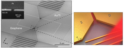
Graphene has extraordinary electro-optic properties and is therefore a promising candidate for monolithic photonic devices such as photodetectors. However, the integration of this atom-thin layer material with bulky photonic components usually results in a weak light–graphene interaction, leading to large device lengths, limiting electro-optic performance. In contrast, here we demonstrate a plasmonic slot graphene photodetector on silicon-on-insulator platform with high responsivity of 0.7 A/W given a just 5 μm short device length. We observe that the maximum photocurrent and, hence, the highest responsivity, scales inversely with the slot width. Using a dual-lithography step, we realize 15 nm narrow slots that show a 30× higher responsivity per unit device-length when compared to photonic graphene photodetectors. Furthermore, we reveal that the back-gated electrostatics is overshadowed by channel-doping contributions induced by the contacts of this ultrashort channel graphene photodetector. This leads to quasi charge neutrality, which explains both the previously unseen offset between the maximum photovoltaic-based photocurrent relative to graphene’s Dirac point and the observed nonambipolar transport characteristics. Such micrometer-compact and absorption-efficient photodetectors allow for short-carrier pathways in next-generation photonic components, while being offering a testbed for studying short-channel carrier physics in graphene optoelectronic devices.
中文翻译:

绝缘体上硅具有高响应性的紧凑型石墨烯等离子缝隙光电探测器
石墨烯具有非凡的电光特性,因此是单片光子器件(例如光电探测器)的有希望的候选者。但是,这种原子薄层材料与笨重的光子组件集成在一起通常会导致弱的光石墨烯相互作用,从而导致器件长度变长,从而限制了电光性能。相比之下,在这里我们演示了在绝缘体上硅平台上的等离子缝隙石墨烯光电探测器,在仅短于5μm的短器件长度下,具有0.7 A / W的高响应度。我们观察到,最大光电流以及因此最高的响应度与缝隙宽度成反比。使用双光刻步骤,我们实现了15 nm的窄缝,与光子石墨烯光电探测器相比,每单元器件长度的响应度提高了30倍。此外,我们揭示了背栅静电被这种超短通道石墨烯光电探测器的触点所诱导的通道掺杂作用所掩盖。这导致准电荷中性,这解释了相对于石墨烯的狄拉克点的最大基于光伏的光电流与观察到的非双极传输特性之间先前看不见的偏移。这种微米级紧凑且吸收效率高的光电探测器可在下一代光子组件中实现短载体路径,同时为研究石墨烯光电器件中的短通道载体物理特性提供了测试平台。这既解释了以前最大的基于光伏的光电流相对于石墨烯的狄拉克点的偏移,也观察到了非双极传输特性。这种微米级紧凑且吸收效率高的光电探测器可在下一代光子组件中实现短载流子路径,同时为研究石墨烯光电器件中的短通道载流子物理特性提供了测试平台。这解释了以前最大的基于光伏的相对于石墨烯的狄拉克点的光电流与未观察到的非双极性传输特性之间的偏移。这种微米级紧凑且吸收效率高的光电探测器可在下一代光子组件中实现短载体路径,同时为研究石墨烯光电器件中的短通道载体物理特性提供了测试平台。
更新日期:2020-02-12
中文翻译:
绝缘体上硅具有高响应性的紧凑型石墨烯等离子缝隙光电探测器
石墨烯具有非凡的电光特性,因此是单片光子器件(例如光电探测器)的有希望的候选者。但是,这种原子薄层材料与笨重的光子组件集成在一起通常会导致弱的光石墨烯相互作用,从而导致器件长度变长,从而限制了电光性能。相比之下,在这里我们演示了在绝缘体上硅平台上的等离子缝隙石墨烯光电探测器,在仅短于5μm的短器件长度下,具有0.7 A / W的高响应度。我们观察到,最大光电流以及因此最高的响应度与缝隙宽度成反比。使用双光刻步骤,我们实现了15 nm的窄缝,与光子石墨烯光电探测器相比,每单元器件长度的响应度提高了30倍。此外,我们揭示了背栅静电被这种超短通道石墨烯光电探测器的触点所诱导的通道掺杂作用所掩盖。这导致准电荷中性,这解释了相对于石墨烯的狄拉克点的最大基于光伏的光电流与观察到的非双极传输特性之间先前看不见的偏移。这种微米级紧凑且吸收效率高的光电探测器可在下一代光子组件中实现短载体路径,同时为研究石墨烯光电器件中的短通道载体物理特性提供了测试平台。这既解释了以前最大的基于光伏的光电流相对于石墨烯的狄拉克点的偏移,也观察到了非双极传输特性。这种微米级紧凑且吸收效率高的光电探测器可在下一代光子组件中实现短载流子路径,同时为研究石墨烯光电器件中的短通道载流子物理特性提供了测试平台。这解释了以前最大的基于光伏的相对于石墨烯的狄拉克点的光电流与未观察到的非双极性传输特性之间的偏移。这种微米级紧凑且吸收效率高的光电探测器可在下一代光子组件中实现短载体路径,同时为研究石墨烯光电器件中的短通道载体物理特性提供了测试平台。


 京公网安备 11010802027423号