Our official English website, www.x-mol.net, welcomes your
feedback! (Note: you will need to create a separate account there.)
Limitation of Current Transport across the Heterojunction in Cu(In,Ga)Se2 Solar Cells Prepared with Alkali Fluoride Postdeposition Treatment
Solar RRL ( IF 6.0 ) Pub Date : 2020-02-10 , DOI: 10.1002/solr.201900560 Alejandra Villanueva-Tovar 1 , Tim Kodalle 1 , Christian A. Kaufmann 1 , Rutger Schlatmann 1, 2 , Reiner Klenk 1
Solar RRL ( IF 6.0 ) Pub Date : 2020-02-10 , DOI: 10.1002/solr.201900560 Alejandra Villanueva-Tovar 1 , Tim Kodalle 1 , Christian A. Kaufmann 1 , Rutger Schlatmann 1, 2 , Reiner Klenk 1
Affiliation
|
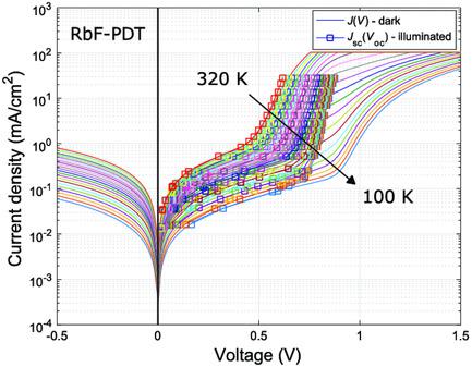
Postdeposition treatments (PDTs) of chalcopyrite absorbers with alkali fluorides have contributed to improving the efficiency of corresponding solar cell devices. However, cells prepared with PDTs also tend to exhibit nonideal current–voltage (J–V) characteristics especially at low temperatures. These include blocking of the forward diode current, saturation of the open‐circuit voltage with respect to temperature, a discrepancy between dark and Jsc (Voc) characteristics, and a crossover between dark and light J–V curves. These are typical observations while measuring the temperature‐dependent J–V characteristics. Herein, the influence of electronic material parameters on the blocking of the current across the heterojunction in numerical simulations is reported. It is shown that a low‐doped ZnO window layer, acceptor defects at the CdS/ZnO interface, or a high band offset at that interface lead to similar nonideal J–V characteristics, suggesting that the carrier density in the buffer layer is a crucial parameter for the current limitation. Connections between the effects of PDT previously reported in literature and the electronic material parameters considered in the numerical model are discussed to explain the nonideal J–V characteristics caused by the PDTs.
中文翻译:

碱性氟化物后沉积法制备的Cu(In,Ga)Se2太阳能电池中跨异质结电流传输的限制
用碱性氟化物对黄铜矿吸收剂进行后沉积处理(PDT)有助于提高相应太阳能电池装置的效率。然而,随着的PDT制备的细胞也倾向于表现出不理想的电流-电压(Ĵ-V尤其在低温下)的特性。这些措施包括阻止正向二极管电流,相对于温度的开路电压饱和,暗和J sc(V oc)特性之间的差异以及暗和亮J–V曲线之间的交叉。这些都是典型的观察结果,同时测量温度依赖性Ĵ-V特征。在此,报道了在数值模拟中电子材料参数对跨异质结的电流阻挡的影响。结果表明,低掺杂的ZnO窗口层,CdS / ZnO界面处的受体缺陷或该界面处的高带偏移会导致类似的非理想J–V特性,这表明缓冲层中的载流子密度至关重要。当前限制的参数。PDT的先前在文献中报道的效果和在数值模型中考虑的电子元件材料的参数之间的连接进行了讨论以解释非理想Ĵ-V引起的PDT特性。
更新日期:2020-02-10
中文翻译:
碱性氟化物后沉积法制备的Cu(In,Ga)Se2太阳能电池中跨异质结电流传输的限制
用碱性氟化物对黄铜矿吸收剂进行后沉积处理(PDT)有助于提高相应太阳能电池装置的效率。然而,随着的PDT制备的细胞也倾向于表现出不理想的电流-电压(Ĵ-V尤其在低温下)的特性。这些措施包括阻止正向二极管电流,相对于温度的开路电压饱和,暗和J sc(V oc)特性之间的差异以及暗和亮J–V曲线之间的交叉。这些都是典型的观察结果,同时测量温度依赖性Ĵ-V特征。在此,报道了在数值模拟中电子材料参数对跨异质结的电流阻挡的影响。结果表明,低掺杂的ZnO窗口层,CdS / ZnO界面处的受体缺陷或该界面处的高带偏移会导致类似的非理想J–V特性,这表明缓冲层中的载流子密度至关重要。当前限制的参数。PDT的先前在文献中报道的效果和在数值模型中考虑的电子元件材料的参数之间的连接进行了讨论以解释非理想Ĵ-V引起的PDT特性。


 京公网安备 11010802027423号