当前位置:
X-MOL 学术
›
Nat. Nanotechnol.
›
论文详情
Our official English website, www.x-mol.net, welcomes your
feedback! (Note: you will need to create a separate account there.)
Graphene-assisted spontaneous relaxation towards dislocation-free heteroepitaxy.
Nature Nanotechnology ( IF 38.1 ) Pub Date : 2020-02-10 , DOI: 10.1038/s41565-020-0633-5 Sang-Hoon Bae 1, 2 , Kuangye Lu 1, 2 , Yimo Han 3 , Sungkyu Kim 1, 2 , Kuan Qiao 1, 2 , Chanyeol Choi 2, 4 , Yifan Nie 5 , Hyunseok Kim 1, 2 , Hyun S Kum 1, 2 , Peng Chen 1, 2 , Wei Kong 1, 2 , Beom-Seok Kang 1, 2 , Chansoo Kim 1, 2 , Jaeyong Lee 1, 2 , Yongmin Baek 6 , Jaewoo Shim 1, 2 , Jinhee Park 7 , Minho Joo 7 , David A Muller 3, 8 , Kyusang Lee 6 , Jeehwan Kim 1, 2, 9
Nature Nanotechnology ( IF 38.1 ) Pub Date : 2020-02-10 , DOI: 10.1038/s41565-020-0633-5 Sang-Hoon Bae 1, 2 , Kuangye Lu 1, 2 , Yimo Han 3 , Sungkyu Kim 1, 2 , Kuan Qiao 1, 2 , Chanyeol Choi 2, 4 , Yifan Nie 5 , Hyunseok Kim 1, 2 , Hyun S Kum 1, 2 , Peng Chen 1, 2 , Wei Kong 1, 2 , Beom-Seok Kang 1, 2 , Chansoo Kim 1, 2 , Jaeyong Lee 1, 2 , Yongmin Baek 6 , Jaewoo Shim 1, 2 , Jinhee Park 7 , Minho Joo 7 , David A Muller 3, 8 , Kyusang Lee 6 , Jeehwan Kim 1, 2, 9
Affiliation
|
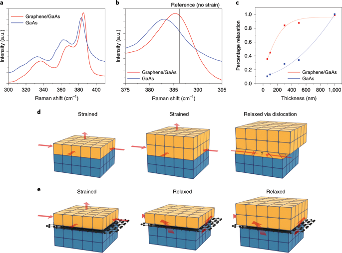
Although conventional homoepitaxy forms high-quality epitaxial layers1-5, the limited set of material systems for commercially available wafers restricts the range of materials that can be grown homoepitaxially. At the same time, conventional heteroepitaxy of lattice-mismatched systems produces dislocations above a critical strain energy to release the accumulated strain energy as the film thickness increases. The formation of dislocations, which severely degrade electronic/photonic device performances6-8, is fundamentally unavoidable in highly lattice-mismatched epitaxy9-11. Here, we introduce a unique mechanism of relaxing misfit strain in heteroepitaxial films that can enable effective lattice engineering. We have observed that heteroepitaxy on graphene-coated substrates allows for spontaneous relaxation of misfit strain owing to the slippery graphene surface while achieving single-crystalline films by reading the atomic potential from the substrate. This spontaneous relaxation technique could transform the monolithic integration of largely lattice-mismatched systems by covering a wide range of the misfit spectrum to enhance and broaden the functionality of semiconductor devices for advanced electronics and photonics.
中文翻译:

石墨烯自发弛豫,实现无位错异质外延。
尽管常规的同质外延形成高质量的外延层1-5,但是用于商业上可获得的晶片的材料系统的有限集合限制了可以同质外延生长的材料的范围。同时,晶格失配系统的传统异质外延在临界应变能以上产生位错,从而随着膜厚度的增加释放出累积的应变能。在高度晶格失配的外延9-11中,不可避免地会形成位错,这会严重降低电子/光子器件的性能6-8。在这里,我们介绍了一种独特的机制,可以缓解异质外延薄膜中的失配应变,从而可以实现有效的晶格工程。我们已经观察到,在石墨烯涂层的基底上的异外延性可以自发地放松由于石墨烯表面光滑而引起的失配应变,同时通过从基底上读取原子电势获得单晶膜。这种自发的弛豫技术可以通过覆盖范围广泛的失配光谱来增强和扩展用于高级电子和光子学的半导体器件的功能,从而转变很大程度上晶格不匹配的系统的单片集成。
更新日期:2020-02-10
中文翻译:
石墨烯自发弛豫,实现无位错异质外延。
尽管常规的同质外延形成高质量的外延层1-5,但是用于商业上可获得的晶片的材料系统的有限集合限制了可以同质外延生长的材料的范围。同时,晶格失配系统的传统异质外延在临界应变能以上产生位错,从而随着膜厚度的增加释放出累积的应变能。在高度晶格失配的外延9-11中,不可避免地会形成位错,这会严重降低电子/光子器件的性能6-8。在这里,我们介绍了一种独特的机制,可以缓解异质外延薄膜中的失配应变,从而可以实现有效的晶格工程。我们已经观察到,在石墨烯涂层的基底上的异外延性可以自发地放松由于石墨烯表面光滑而引起的失配应变,同时通过从基底上读取原子电势获得单晶膜。这种自发的弛豫技术可以通过覆盖范围广泛的失配光谱来增强和扩展用于高级电子和光子学的半导体器件的功能,从而转变很大程度上晶格不匹配的系统的单片集成。


 京公网安备 11010802027423号