Nature Materials ( IF 41.2 ) Pub Date : 2020-02-03 , DOI: 10.1038/s41563-019-0601-3 Nicolas Ubrig 1, 2 , Evgeniy Ponomarev 1, 2 , Johanna Zultak 3, 4, 5 , Daniil Domaretskiy 1, 2 , Viktor Zólyomi 3 , Daniel Terry 3, 4, 5 , James Howarth 3, 4, 5 , Ignacio Gutiérrez-Lezama 1, 2 , Alexander Zhukov 3, 4, 5 , Zakhar R Kudrynskyi 6 , Zakhar D Kovalyuk 7 , Amalia Patané 6 , Takashi Taniguchi 8 , Kenji Watanabe 8 , Roman V Gorbachev 3, 4, 5 , Vladimir I Fal'ko 3, 4, 5 , Alberto F Morpurgo 1, 2
|
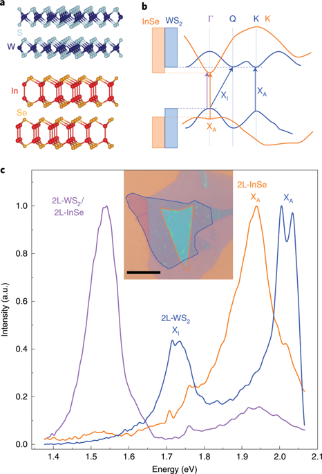
Van der Waals (vdW) interfaces based on 2D materials are promising for optoelectronics, as interlayer transitions between different compounds allow tailoring of the spectral response over a broad range. However, issues such as lattice mismatch or a small misalignment of the constituent layers can drastically suppress electron–photon coupling for these interlayer transitions. Here, we engineered type-II interfaces by assembling atomically thin crystals that have the bottom of the conduction band and the top of the valence band at the Γ point, and thus avoid any momentum mismatch. We found that these van der Waals interfaces exhibit radiative optical transitions irrespective of the lattice constant, the rotational and/or translational alignment of the two layers or whether the constituent materials are direct or indirect gap semiconductors. Being robust and of general validity, our results broaden the scope of future optoelectronics device applications based on two-dimensional materials.
中文翻译:
广谱光电子学的范德华界面设计
基于 2D 材料的范德华 (vdW) 界面有望用于光电子学,因为不同化合物之间的层间跃迁允许在宽范围内调整光谱响应。然而,诸如晶格失配或组成层的小错位等问题可以极大地抑制这些层间跃迁的电子 - 光子耦合。在这里,我们通过组装在Γ点处具有导带底部和价带顶部的原子薄晶体来设计II型界面,从而避免任何动量不匹配。我们发现无论晶格常数、两层的旋转和/或平移排列或组成材料是直接还是间接间隙半导体,这些范德华界面都表现出辐射光学跃迁。


 京公网安备 11010802027423号