当前位置:
X-MOL 学术
›
Solid State Sci.
›
论文详情
Our official English website, www.x-mol.net, welcomes your
feedback! (Note: you will need to create a separate account there.)
Physical characterization of CuO thin films obtained by thermal oxidation of vacuum evaporated Cu
Solid State Sciences ( IF 3.4 ) Pub Date : 2020-03-01 , DOI: 10.1016/j.solidstatesciences.2020.106147 R. Djebian , B. Boudjema , A. Kabir , C. Sedrati
Solid State Sciences ( IF 3.4 ) Pub Date : 2020-03-01 , DOI: 10.1016/j.solidstatesciences.2020.106147 R. Djebian , B. Boudjema , A. Kabir , C. Sedrati
|
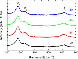
Abstract In this work, CuO thin films were obtained from the oxidation, at 300 °C, of vacuum evaporated Cu thin films. The XRD patterns revealed the polycrystalline structure of the monoclinic CuO with a preferential orientation along the (111) planes. The direct formation of CuO was confirmed by the Raman spectroscopy. The variation of the crystallographic parameters as a function of the heating time was interpreted by a collective action of intrinsic and thermal stresses. The grain growth of the CuO films was found to be controlled by the surface diffusion of pores. SEM image show the formation of homogenous structure and the O/Cu atomic ratio varied between 0.8 and 1.15 reflecting the nonstoichiometry of CuO films. The UV–visible spectroscopy and the electrical measurements revealed that the band gap energy and the electrical resistivity variations were influenced by the crystallite size and the nonstoichiometry of the CuO films. The band gap energy varied between 1.73 and 2 eV while the electrical resistivity varied between 2.7 and 6.5 kΩ cm.
中文翻译:

真空蒸发铜热氧化得到的氧化铜薄膜的物理表征
摘要 在这项工作中,CuO 薄膜是通过在 300 °C 下对真空蒸发的 Cu 薄膜进行氧化而获得的。XRD图谱揭示了单斜CuO的多晶结构,沿(111)面具有优先取向。拉曼光谱证实了CuO的直接形成。作为加热时间的函数的晶体学参数的变化通过内应力和热应力的集体作用来解释。发现CuO薄膜的晶粒生长受孔的表面扩散控制。SEM 图像显示均匀结构的形成和 O/Cu 原子比在 0.8 和 1.15 之间变化,反映了 CuO 薄膜的非化学计量。紫外可见光谱和电学测量表明,带隙能量和电阻率变化受微晶尺寸和 CuO 薄膜的非化学计量的影响。带隙能量在 1.73 和 2 eV 之间变化,而电阻率在 2.7 和 6.5 kΩ cm 之间变化。
更新日期:2020-03-01
中文翻译:
真空蒸发铜热氧化得到的氧化铜薄膜的物理表征
摘要 在这项工作中,CuO 薄膜是通过在 300 °C 下对真空蒸发的 Cu 薄膜进行氧化而获得的。XRD图谱揭示了单斜CuO的多晶结构,沿(111)面具有优先取向。拉曼光谱证实了CuO的直接形成。作为加热时间的函数的晶体学参数的变化通过内应力和热应力的集体作用来解释。发现CuO薄膜的晶粒生长受孔的表面扩散控制。SEM 图像显示均匀结构的形成和 O/Cu 原子比在 0.8 和 1.15 之间变化,反映了 CuO 薄膜的非化学计量。紫外可见光谱和电学测量表明,带隙能量和电阻率变化受微晶尺寸和 CuO 薄膜的非化学计量的影响。带隙能量在 1.73 和 2 eV 之间变化,而电阻率在 2.7 和 6.5 kΩ cm 之间变化。


 京公网安备 11010802027423号