当前位置:
X-MOL 学术
›
Ultramicroscopy
›
论文详情
Our official English website, www.x-mol.net, welcomes your
feedback! (Note: you will need to create a separate account there.)
Variable Voltage Electron Microscopy: Toward Atom-by-Atom Fabrication in 2D Materials
Ultramicroscopy ( IF 2.1 ) Pub Date : 2020-04-01 , DOI: 10.1016/j.ultramic.2020.112949 Ondrej Dyck 1 , Stephen Jesse 1 , Niklas Delby 2 , Sergei V Kalinin 1 , Andrew R Lupini 1
Ultramicroscopy ( IF 2.1 ) Pub Date : 2020-04-01 , DOI: 10.1016/j.ultramic.2020.112949 Ondrej Dyck 1 , Stephen Jesse 1 , Niklas Delby 2 , Sergei V Kalinin 1 , Andrew R Lupini 1
Affiliation
|
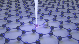
The precisely focused electron beam (e-beam) in scanning transmission electron microscopy has been found to be a versatile tool for patterning matter on the atomic level and enabling atom-by-atom fabrication, however, beam-induced phenomena are known to be extremely sensitive to the e-beam energy and are closely correlated with the proximity of the knock-on threshold. Here we provide a method to control the energy transferred to the sample while facilitating much faster changes in accelerating voltages by maintaining a nearly constant temperature in the electron microscope lenses. We use this method to demonstrate in-situ nano-milling of a graphene film followed rapidly by "gentler" imaging at lower energy. Additionally, the insertion and controlled movement of silicon dopants in graphene is demonstrated by employing a different e-beam energy during each process. We believe the incorporation of variable e-beam energy will broaden the potential for atomic scale e-beam fabrication.
中文翻译:

变压电子显微镜:在二维材料中逐个原子地制造
扫描透射电子显微镜中精确聚焦的电子束 (e-beam) 已被发现是一种通用工具,可用于在原子水平上对物质进行图案化并实现逐个原子的制造,然而,众所周知,电子束诱导现象极其严重。对电子束能量敏感,并与爆震阈值的接近度密切相关。在这里,我们提供了一种方法来控制转移到样品的能量,同时通过在电子显微镜镜头中保持几乎恒定的温度来促进加速电压的更快变化。我们使用这种方法来演示石墨烯薄膜的原位纳米研磨,然后在较低能量下快速进行“温和”成像。此外,通过在每个过程中使用不同的电子束能量,证明了硅掺杂剂在石墨烯中的插入和受控移动。我们相信可变电子束能量的结合将拓宽原子级电子束制造的潜力。
更新日期:2020-04-01
中文翻译:
变压电子显微镜:在二维材料中逐个原子地制造
扫描透射电子显微镜中精确聚焦的电子束 (e-beam) 已被发现是一种通用工具,可用于在原子水平上对物质进行图案化并实现逐个原子的制造,然而,众所周知,电子束诱导现象极其严重。对电子束能量敏感,并与爆震阈值的接近度密切相关。在这里,我们提供了一种方法来控制转移到样品的能量,同时通过在电子显微镜镜头中保持几乎恒定的温度来促进加速电压的更快变化。我们使用这种方法来演示石墨烯薄膜的原位纳米研磨,然后在较低能量下快速进行“温和”成像。此外,通过在每个过程中使用不同的电子束能量,证明了硅掺杂剂在石墨烯中的插入和受控移动。我们相信可变电子束能量的结合将拓宽原子级电子束制造的潜力。


 京公网安备 11010802027423号