Our official English website, www.x-mol.net, welcomes your
feedback! (Note: you will need to create a separate account there.)
Higher‐Order Topological States in Surface‐Wave Photonic Crystals
Advanced Science ( IF 14.3 ) Pub Date : 2020-01-27 , DOI: 10.1002/advs.201902724 Li Zhang 1, 2 , Yihao Yang 3, 4 , Zhi-Kang Lin 5 , Pengfei Qin 1, 2 , Qiaolu Chen 1, 2 , Fei Gao 1, 2 , Erping Li 1, 2 , Jian-Hua Jiang 5 , Baile Zhang 3, 4 , Hongsheng Chen 1, 2
Advanced Science ( IF 14.3 ) Pub Date : 2020-01-27 , DOI: 10.1002/advs.201902724 Li Zhang 1, 2 , Yihao Yang 3, 4 , Zhi-Kang Lin 5 , Pengfei Qin 1, 2 , Qiaolu Chen 1, 2 , Fei Gao 1, 2 , Erping Li 1, 2 , Jian-Hua Jiang 5 , Baile Zhang 3, 4 , Hongsheng Chen 1, 2
Affiliation
|
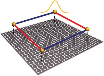
Photonic topological states have revolutionized the understanding of the propagation and scattering of light. The recent discovery of higher‐order photonic topological insulators opens an emergent horizon for 0D topological corner states. However, the previous realizations of higher‐order topological insulators in electromagnetic‐wave systems suffer from either a limited operational frequency range due to the lumped components involved or a bulky structure with a large footprint, which are unfavorable for achieving compact photonic devices. To overcome these limitations, a planar surface‐wave photonic crystal realization of 2D higher‐order topological insulators is hereby demonstrated experimentally. The surface‐wave photonic crystals exhibit a very large bulk bandgap (a bandwidth of 28%) due to multiple Bragg scatterings and host 1D gapped edge states described by massive Dirac equations. The topology of those higher‐dimensional photonic bands leads to the emergence of in‐gap 0D corner states, which provide a route toward robust cavity modes for scalable compact photonic devices.
中文翻译:

表面波光子晶体中的高阶拓扑态
光子拓扑态彻底改变了对光传播和散射的理解。最近发现的高阶光子拓扑绝缘体为 0D 拓扑角态开辟了新的视野。然而,先前在电磁波系统中实现的高阶拓扑绝缘体要么由于涉及的集总元件而受到有限的工作频率范围的限制,要么由于占地面积大的笨重结构,这不利于实现紧凑的光子器件。为了克服这些限制,特此通过实验证明了二维高阶拓扑绝缘体的平面表面波光子晶体实现。由于多重布拉格散射和大量狄拉克方程描述的一维带隙边缘态,表面波光子晶体表现出非常大的体带隙(带宽为 28%)。这些高维光子带的拓扑结构导致了带隙内 0D 角态的出现,这为可扩展的紧凑型光子器件提供了一条通往稳健腔模式的途径。
更新日期:2020-01-27
中文翻译:
表面波光子晶体中的高阶拓扑态
光子拓扑态彻底改变了对光传播和散射的理解。最近发现的高阶光子拓扑绝缘体为 0D 拓扑角态开辟了新的视野。然而,先前在电磁波系统中实现的高阶拓扑绝缘体要么由于涉及的集总元件而受到有限的工作频率范围的限制,要么由于占地面积大的笨重结构,这不利于实现紧凑的光子器件。为了克服这些限制,特此通过实验证明了二维高阶拓扑绝缘体的平面表面波光子晶体实现。由于多重布拉格散射和大量狄拉克方程描述的一维带隙边缘态,表面波光子晶体表现出非常大的体带隙(带宽为 28%)。这些高维光子带的拓扑结构导致了带隙内 0D 角态的出现,这为可扩展的紧凑型光子器件提供了一条通往稳健腔模式的途径。


 京公网安备 11010802027423号