Nature Photonics ( IF 32.3 ) Pub Date : 2020-01-27 , DOI: 10.1038/s41566-019-0580-6 Christian Heide , Martin Hauck , Takuya Higuchi , Jürgen Ristein , Lothar Ley , Heiko B. Weber , Peter Hommelhoff
|
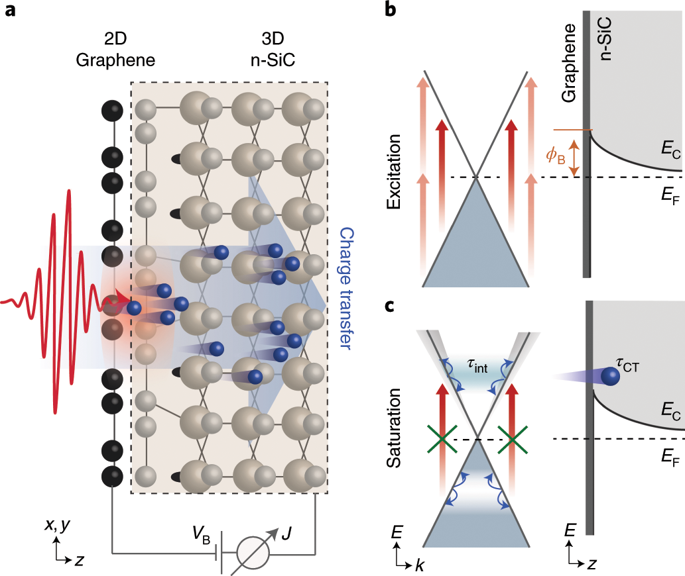
The photoelectric effect has a sister process relevant in optoelectronics called internal photoemission1,2,3. Here an electron is photoemitted from a metal into a semiconductor4,5. While the photoelectric effect takes place within less than 100 attoseconds (1 as = 10−18 seconds)6,7, the attosecond timescale has so far not been measured for internal photoemission. Based on the new method CHArge transfer time MEasurement via Laser pulse duration-dependent saturation fluEnce determinatiON—CHAMELEON—we show that the atomically thin semimetal graphene coupled to bulk silicon carbide, forming a Schottky junction, allows charge transfer times as fast as (300 ± 200) as. These results are supported by a simple quantum mechanical model simulation. With the obtained cut-off bandwidth of 3.3 PHz (1 PHz = 1015 Hz) for the charge transfer rate, this semimetal/semiconductor interface represents a functional solid-state interface offering the speed and design space required for future light-wave signal processing.
中文翻译:
亚秒级快速内部光发射
光电效应具有与光电相关的姐妹过程,称为内部光发射1,2,3。在这里,电子从金属光发射到半导体4,5中。光电效应发生在不到100阿秒内(1等于10 -18秒)6,7,到目前为止,尚未测量内部光发射的秒级时标。基于新方法,通过与激光脉冲持续时间有关的饱和通量测定(CHAMELEON)来测量电荷转移时间,我们证明,原子薄的半金属石墨烯与块状碳化硅偶联形成了肖特基结,电荷转移时间快于(300± 200)。这些结果得到简单的量子力学模型仿真的支持。由于获得 的电荷传输速率的截止带宽为3.3 PHz(1 PHz = 10 15 Hz),因此这种半金属/半导体接口代表了一种功能性的固态接口,可提供未来光波信号处理所需的速度和设计空间。


 京公网安备 11010802027423号