Our official English website, www.x-mol.net, welcomes your
feedback! (Note: you will need to create a separate account there.)
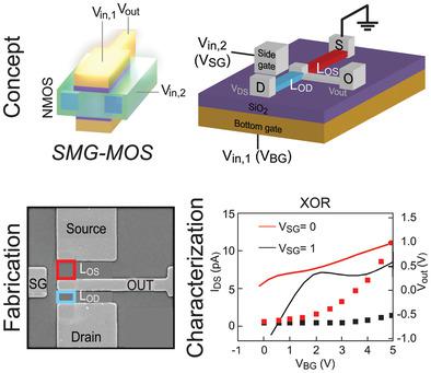
Bottom‐Gate Approach for All Basic Logic Gates Implementation by a Single‐Type IGZO‐Based MOS Transistor with Reduced Footprint
Advanced Science ( IF 14.3 ) Pub Date : 2020-01-24 , DOI: 10.1002/advs.201901224 Shaocheng Qi 1, 2 , Joao Cunha 2, 3, 4 , Tian-Long Guo 2, 3 , Peiqin Chen 2 , Remo Proietti Zaccaria 2, 3, 5 , Mingzhi Dai 2
Advanced Science ( IF 14.3 ) Pub Date : 2020-01-24 , DOI: 10.1002/advs.201901224 Shaocheng Qi 1, 2 , Joao Cunha 2, 3, 4 , Tian-Long Guo 2, 3 , Peiqin Chen 2 , Remo Proietti Zaccaria 2, 3, 5 , Mingzhi Dai 2
Affiliation
|
Logic functions are the key backbone in electronic circuits for computing applications. Complementary metal‐oxide‐semiconductor (CMOS) logic gates, with both n‐type and p‐type channel transistors, have been to date the dominant building blocks of logic circuitry as they carry obvious advantages over other technologies. Important physical limits are however starting to arise, as the transistor‐processing technology has begun to meet scaling‐down difficulties. To address this issue, there is the crucial need for a next‐generation electronics era based on new concepts and designs. In this respect, a single‐type channel multigate MOS transistor (SMG‐MOS) is introduced holding the two important aspects of processing adaptability and low static dissipation of CMOS. Furthermore, the SMG‐MOS approach strongly reduces the footprint down to 40% or even less area needed for current CMOS logic function in the same processing technology node. Logic NAND, NOT, AND, NOR, and OR gates, which typically require a large number of CMOS transistors, can be realized by a single SMG‐MOS transistor. Two functional examples of SMG‐MOS are reported here with their analysis based both on simulations and experiments. The results strongly suggest that SMG‐MOS can represent a facile approach to scale down complex integrated circuits, enabling design flexibility and production rates ramp‐up.
中文翻译:

通过基于 IGZO 的单型 MOS 晶体管实现所有基本逻辑门的底栅方法,占用空间更小
逻辑功能是计算应用电子电路的关键支柱。具有 n 型和 p 型沟道晶体管的互补金属氧化物半导体 (CMOS) 逻辑门迄今为止已成为逻辑电路的主要构建模块,因为它们比其他技术具有明显的优势。然而,随着晶体管处理技术开始遇到缩小尺寸的困难,重要的物理限制开始出现。为了解决这个问题,迫切需要基于新概念和设计的下一代电子时代。在这方面,引入了单型沟道多栅MOS晶体管(SMG-MOS),它兼顾了CMOS的加工适应性和低静态耗散两个重要方面。此外,SMG-MOS 方法大大减少了相同处理技术节点中当前 CMOS 逻辑功能所需面积的 40% 甚至更少。逻辑 NAND、NOT、AND、NOR 和 OR 门通常需要大量 CMOS 晶体管,但可以通过单个 SMG-MOS 晶体管来实现。这里报告了 SMG-MOS 的两个功能示例以及基于模拟和实验的分析。结果强烈表明,SMG-MOS 可以代表一种缩小复杂集成电路规模的简便方法,从而实现设计灵活性和生产率提升。
更新日期:2020-01-24
中文翻译:
通过基于 IGZO 的单型 MOS 晶体管实现所有基本逻辑门的底栅方法,占用空间更小
逻辑功能是计算应用电子电路的关键支柱。具有 n 型和 p 型沟道晶体管的互补金属氧化物半导体 (CMOS) 逻辑门迄今为止已成为逻辑电路的主要构建模块,因为它们比其他技术具有明显的优势。然而,随着晶体管处理技术开始遇到缩小尺寸的困难,重要的物理限制开始出现。为了解决这个问题,迫切需要基于新概念和设计的下一代电子时代。在这方面,引入了单型沟道多栅MOS晶体管(SMG-MOS),它兼顾了CMOS的加工适应性和低静态耗散两个重要方面。此外,SMG-MOS 方法大大减少了相同处理技术节点中当前 CMOS 逻辑功能所需面积的 40% 甚至更少。逻辑 NAND、NOT、AND、NOR 和 OR 门通常需要大量 CMOS 晶体管,但可以通过单个 SMG-MOS 晶体管来实现。这里报告了 SMG-MOS 的两个功能示例以及基于模拟和实验的分析。结果强烈表明,SMG-MOS 可以代表一种缩小复杂集成电路规模的简便方法,从而实现设计灵活性和生产率提升。


 京公网安备 11010802027423号