Nano Energy ( IF 16.8 ) Pub Date : 2020-01-16 , DOI: 10.1016/j.nanoen.2020.104495 Julie Dréon , Quentin Jeangros , Jean Cattin , Jan Haschke , Luca Antognini , Christophe Ballif , Mathieu Boccard
|
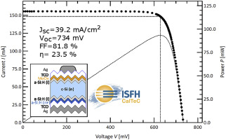
Interest in silicon heterojunction solar cells is growing due to their manufacturing simplicity and record efficiencies. However, a significant limitation of these devices still stems from parasitic light absorption in the amorphous silicon layers. This can be mitigated by replacing the traditional (p) and (n) doped amorphous silicon selective layers by other materials. While promising results have been achieved using molybdenum oxide (MoOx) as a front-side hole-selective layer, charge transport mechanisms in that contact stack have remained elusive and device efficiencies below predictions. We carefully analyze the influence of the MoOx and intrinsic a-Si:H thicknesses on current-voltage properties and discuss transport and performance-loss mechanisms. In particular, we find that thinning down the MoOx and (i)a-Si:H layers (down to 4 nm and 6 nm respectively) mitigates parasitic sub-bandgap MoOx optical absorption and drastically enhances charge transport, while still providing excellent passivation and selectivity. High-resolution transmission microscopy reveals that such thin MoOx layer remains continuous and, while slightly sub-stoechiometric, exhibits a chemistry close to MoO3. A screen-printed device reaching a certified efficiency of 23.5% and a fill factor of 81.8% is demonstrated, bridging the gap with traditional Si-based contacts and demonstrating that dopant-free selective contacts can rival traditional approaches.
中文翻译:
使用氧化钼作为空穴选择接触的23.5%效率的硅异质结硅太阳能电池
由于硅异质结太阳能电池的制造简单性和创纪录的效率,人们对其的兴趣正在增长。然而,这些器件的显着局限性仍然来自于非晶硅层中的寄生光吸收。这可以通过用其他材料代替传统的(p)和(n)掺杂的非晶硅选择层来缓解。尽管使用氧化钼(MoO x)作为正面空穴选择层已经获得了可喜的结果,但该接触堆叠中的电荷传输机制仍然难以捉摸,器件效率也低于预期。我们仔细分析MoO x的影响以及固有的a-Si:H厚度对电流-电压特性的影响,并讨论了传输和性能损失的机制。特别是,我们发现减薄MoO x和(i)a-Si:H层(分别减小至4 nm和6 nm)可减轻寄生带隙MoO x的光学吸收并显着增强电荷传输,同时仍提供出色的钝化和选择性。高分辨率透射显微镜显示,这种薄的MoO x层保持连续,虽然略低于化学计量,但化学性质接近MoO 3。展示了一种丝网印刷设备,该设备达到了23.5%的认证效率和81.8%的填充系数,弥合了传统的基于Si的触点之间的空白,并证明了无掺杂的选择性触点可以与传统方法相媲美。


 京公网安备 11010802027423号