当前位置:
X-MOL 学术
›
Adv. Mater.
›
论文详情
Our official English website, www.x-mol.net, welcomes your
feedback! (Note: you will need to create a separate account there.)
Ultrafast Electrochemical Synthesis of Defect‐Free In2Se3 Flakes for Large‐Area Optoelectronics
Advanced Materials ( IF 27.4 ) Pub Date : 2020-01-15 , DOI: 10.1002/adma.201907244 Huanhuan Shi 1 , Mengmeng Li 1, 2, 3 , Ali Shaygan Nia 1 , Mingchao Wang 1 , SangWook Park 1 , Zhen Zhang 1 , Martin R. Lohe 1 , Sheng Yang 1 , Xinliang Feng 1
Advanced Materials ( IF 27.4 ) Pub Date : 2020-01-15 , DOI: 10.1002/adma.201907244 Huanhuan Shi 1 , Mengmeng Li 1, 2, 3 , Ali Shaygan Nia 1 , Mingchao Wang 1 , SangWook Park 1 , Zhen Zhang 1 , Martin R. Lohe 1 , Sheng Yang 1 , Xinliang Feng 1
Affiliation
|
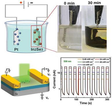
Because of its thickness‐dependent direct bandgap and exceptional optoelectronic properties, indium(III) selenide (In2Se3) has emerged as an important semiconductor for electronics and optoelectronics. However, the scalable synthesis of defect‐free In2Se3 flakes remains a significant barrier for its practical applications. Here, a facile electrochemical strategy is presented for the ultrafast delamination of bulk layered In2Se3 crystals in nonaqueous media, resulting in high‐yield (83%) production of defect‐free In2Se3 flakes with large lateral size (up to 26 µm). The intercalation of tetrahexylammonium (THA+) ions mainly creates stage‐3 intercalated compounds in which every three layers of In2Se3 are occupied by one layer of THA molecules. The subsequent exfoliation leads to a majority of trilayer In2Se3 nanosheets. As a proof of concept, solution‐processed, large‐area (400 µm × 20 µm) thin‐film photodetectors embedded with the exfoliated In2Se3 flakes reveal ultrafast response time with a rise and decay of 41 and 39 ms, respectively, and efficient responsivity (1 mA W−1). Such performance surpasses most of the state‐of‐the‐art thin‐film photodetectors based on transition metal dichalcogenides.
中文翻译:

超快电化学合成用于大面积光电的无缺陷In2Se3薄片
由于其依赖于厚度的直接带隙和出色的光电性能,硒化铟(III)(In 2 Se 3)已成为电子和光电领域的重要半导体。但是,无缺陷的In 2 Se 3薄片的可扩展合成仍然是其实际应用的主要障碍。在此,提出了一种简便的电化学策略,用于在非水介质中超快速分层散装的In 2 Se 3晶体,从而导致高产率(83%)的无缺陷In 2 Se 3薄片的大尺寸生产(最大26 µm)。四己基铵(THA +)离子主要产生3期插层化合物,其中每三层In 2 Se 3被一层THA分子占据。随后的剥落导致大部分三层In 2 Se 3纳米片。作为概念证明,嵌入剥离的In 2 Se 3薄片的固溶处理大面积(400 µm×20 µm)薄膜光电探测器显示出超快的响应时间,分别具有41 ms和39 ms的上升和下降。和高响应度(1 mA W -1)。这样的性能超过了大多数基于过渡金属二卤化物的最先进的薄膜光电探测器。
更新日期:2020-02-24
中文翻译:
超快电化学合成用于大面积光电的无缺陷In2Se3薄片
由于其依赖于厚度的直接带隙和出色的光电性能,硒化铟(III)(In 2 Se 3)已成为电子和光电领域的重要半导体。但是,无缺陷的In 2 Se 3薄片的可扩展合成仍然是其实际应用的主要障碍。在此,提出了一种简便的电化学策略,用于在非水介质中超快速分层散装的In 2 Se 3晶体,从而导致高产率(83%)的无缺陷In 2 Se 3薄片的大尺寸生产(最大26 µm)。四己基铵(THA +)离子主要产生3期插层化合物,其中每三层In 2 Se 3被一层THA分子占据。随后的剥落导致大部分三层In 2 Se 3纳米片。作为概念证明,嵌入剥离的In 2 Se 3薄片的固溶处理大面积(400 µm×20 µm)薄膜光电探测器显示出超快的响应时间,分别具有41 ms和39 ms的上升和下降。和高响应度(1 mA W -1)。这样的性能超过了大多数基于过渡金属二卤化物的最先进的薄膜光电探测器。


 京公网安备 11010802027423号