当前位置:
X-MOL 学术
›
Laser Photonics Rev.
›
论文详情
Our official English website, www.x-mol.net, welcomes your
feedback! (Note: you will need to create a separate account there.)
Fused Silica with Embedded 2D‐Like Ag Nanoparticle Monolayer: Tunable Saturable Absorbers by Interparticle Spacing Manipulation
Laser & Photonics Reviews ( IF 9.8 ) Pub Date : 2020-01-13 , DOI: 10.1002/lpor.201900302 Rang Li 1 , Chi Pang 1 , Ziqi Li 1 , Ming Yang 2 , Hiroshi Amekura 3 , Ningning Dong 4 , Jun Wang 4 , Feng Ren 5 , Qiang Wu 6 , Feng Chen 1
Laser & Photonics Reviews ( IF 9.8 ) Pub Date : 2020-01-13 , DOI: 10.1002/lpor.201900302 Rang Li 1 , Chi Pang 1 , Ziqi Li 1 , Ming Yang 2 , Hiroshi Amekura 3 , Ningning Dong 4 , Jun Wang 4 , Feng Ren 5 , Qiang Wu 6 , Feng Chen 1
Affiliation
|
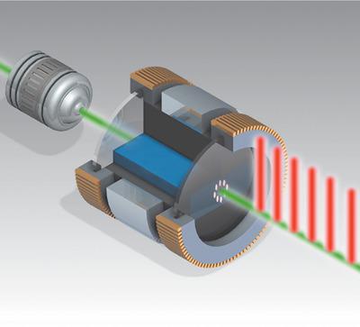
Saturable absorbers are key elements for generation of ultrafast laser pulses. The commercially available semiconductor saturable absorber mirrors are wavelength sensitive and with complex fabrication process and high cost. Fused silica is one of the basic materials for various optical applications. Plasmonic nanoparticles can be used to efficiently modulate the optical properties of dielectric materials owing to the enhanced field effects based on localized surface plasmonic resonance. Ion implantation is a direct technique to synthesize plasmonic nanoparticles inside dielectric materials, which can simultaneously tailor the optical nonlinearity of substrates significantly. In this work, Ag ion implantation into fused silica with tunable interparticle spacing is used to generate broadband optical nonlinearities and to endow silica with ultrafast saturable absorption property. This ion implantation forms a 2D‐like Ag nanoparticle monolayer buried inside fused silica wafer. The fused silica with embedded 2D‐like Ag nanoparticle monolayer is further applied as a new saturable absorber to generate ultrafast laser pulses with pulse duration of 27 ps and repetition rate of 6.5 GHz through the passive mode‐locking process. This work opens up a new route to develop low‐cost, highly stable saturable absorbers, and offers the possibility to build novel silica‐based photonic systems through nanoparticle spacing manipulation.
中文翻译:

具有嵌入式2D类银纳米颗粒单层的熔融石英:通过颗粒间间距操纵可调节的饱和吸收剂
饱和吸收剂是产生超快激光脉冲的关键元素。市售的半导体可饱和吸收镜对波长敏感并且制造工艺复杂且成本高。熔融二氧化硅是用于各种光学应用的基本材料之一。由于基于局部表面等离子体共振的增强的场效应,等离子纳米粒子可用于有效地调节介电材料的光学特性。离子注入是一种在电介质材料内部合成等离子体纳米粒子的直接技术,可以同时显着调整基板的光学非线性。在这项工作中 将Ag离子注入到具有可调粒子间间距的熔融石英中可产生宽带光学非线性,并使二氧化硅具有超快的饱和吸收特性。这种离子注入形成了一个2D状的Ag纳米颗粒单层,埋在熔融石英晶片内部。具有嵌入式2D状Ag纳米粒子单层的熔融石英还被用作一种新型的可饱和吸收体,通过无源锁模过程产生脉冲持续时间为27 ps,重复频率为6.5 GHz的超快激光脉冲。这项工作为开发低成本,高稳定性的可饱和吸收剂开辟了一条新途径,并为通过纳米粒子间距操纵构建新型的基于二氧化硅的光子系统提供了可能性。这种离子注入形成了一个2D状的Ag纳米颗粒单层,埋在熔融石英晶片内部。具有嵌入式2D状Ag纳米粒子单层的熔融石英还被用作一种新型的可饱和吸收体,通过无源锁模过程产生脉冲持续时间为27 ps,重复频率为6.5 GHz的超快激光脉冲。这项工作为开发低成本,高稳定性的可饱和吸收剂开辟了一条新途径,并为通过纳米粒子间距操纵构建新型的基于二氧化硅的光子系统提供了可能性。这种离子注入形成了一个2D状的Ag纳米颗粒单层,埋在熔融石英晶片内部。具有嵌入式2D状Ag纳米粒子单层的熔融石英还被用作一种新型的可饱和吸收体,通过无源锁模过程产生脉冲持续时间为27 ps,重复频率为6.5 GHz的超快激光脉冲。这项工作为开发低成本,高稳定性的可饱和吸收剂开辟了一条新途径,并为通过纳米粒子间距操纵构建新型的基于二氧化硅的光子系统提供了可能性。
更新日期:2020-01-13
中文翻译:
具有嵌入式2D类银纳米颗粒单层的熔融石英:通过颗粒间间距操纵可调节的饱和吸收剂
饱和吸收剂是产生超快激光脉冲的关键元素。市售的半导体可饱和吸收镜对波长敏感并且制造工艺复杂且成本高。熔融二氧化硅是用于各种光学应用的基本材料之一。由于基于局部表面等离子体共振的增强的场效应,等离子纳米粒子可用于有效地调节介电材料的光学特性。离子注入是一种在电介质材料内部合成等离子体纳米粒子的直接技术,可以同时显着调整基板的光学非线性。在这项工作中 将Ag离子注入到具有可调粒子间间距的熔融石英中可产生宽带光学非线性,并使二氧化硅具有超快的饱和吸收特性。这种离子注入形成了一个2D状的Ag纳米颗粒单层,埋在熔融石英晶片内部。具有嵌入式2D状Ag纳米粒子单层的熔融石英还被用作一种新型的可饱和吸收体,通过无源锁模过程产生脉冲持续时间为27 ps,重复频率为6.5 GHz的超快激光脉冲。这项工作为开发低成本,高稳定性的可饱和吸收剂开辟了一条新途径,并为通过纳米粒子间距操纵构建新型的基于二氧化硅的光子系统提供了可能性。这种离子注入形成了一个2D状的Ag纳米颗粒单层,埋在熔融石英晶片内部。具有嵌入式2D状Ag纳米粒子单层的熔融石英还被用作一种新型的可饱和吸收体,通过无源锁模过程产生脉冲持续时间为27 ps,重复频率为6.5 GHz的超快激光脉冲。这项工作为开发低成本,高稳定性的可饱和吸收剂开辟了一条新途径,并为通过纳米粒子间距操纵构建新型的基于二氧化硅的光子系统提供了可能性。这种离子注入形成了一个2D状的Ag纳米颗粒单层,埋在熔融石英晶片内部。具有嵌入式2D状Ag纳米粒子单层的熔融石英还被用作一种新型的可饱和吸收体,通过无源锁模过程产生脉冲持续时间为27 ps,重复频率为6.5 GHz的超快激光脉冲。这项工作为开发低成本,高稳定性的可饱和吸收剂开辟了一条新途径,并为通过纳米粒子间距操纵构建新型的基于二氧化硅的光子系统提供了可能性。


 京公网安备 11010802027423号