当前位置:
X-MOL 学术
›
ACS Appl. Electron. Mater.
›
论文详情
Our official English website, www.x-mol.net, welcomes your
feedback! (Note: you will need to create a separate account there.)
Fermi-Level Engineering of Atomic Layer-Deposited Zinc Oxide Thin Films for a Vertically Stacked Inverter
ACS Applied Electronic Materials ( IF 4.3 ) Pub Date : 2020-01-23 , DOI: 10.1021/acsaelm.9b00785 Minho Yoon 1 , Jongdae Park 1 , Dai Cuong Tran 1 , Myung Mo Sung 1
ACS Applied Electronic Materials ( IF 4.3 ) Pub Date : 2020-01-23 , DOI: 10.1021/acsaelm.9b00785 Minho Yoon 1 , Jongdae Park 1 , Dai Cuong Tran 1 , Myung Mo Sung 1
Affiliation
|
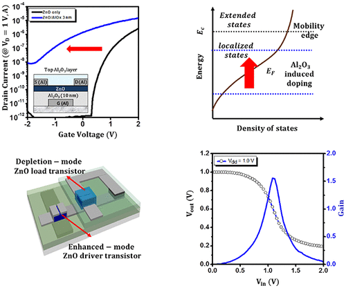
We report here atomic layer-deposited ZnO FETs and an effective electron doping method based on Al2O3 layer for high-performance transistors and its circuit application. Through the atomic layer deposition, an ultrathin and flat ZnO film (5 nm) has been deposited successfully where our ZnO FETs initially show n-type enhancement-mode transfer characteristics. The threshold voltage and the electron field-effect mobility of the device are 42 V and 2.8 cm2 V–1 s–1, respectively. After the deposition of the top Al2O3 layer, our ZnO FETs exhibit depletion-mode transfer characteristics with enhanced mobility. The threshold voltage (Vth) shifts to −38 V and the electron field-effect mobility increases by a factor of 2. Analyzed by a four-point probe and Hall and temperature-variable current–voltage measurements, Al2O3-induced doping is considered the main reason for the noticeable changes by minimizing the trap states in our ZnO films. Furthermore, a vertically stacked low-voltage n-type ZnO inverter was successfully fabricated utilizing the enhancement- and depletion-mode ZnO FETs with a voltage gain of ∼1.5 at low supplied voltage. We thus conclude that the atomic layer-deposited ZnO FETs with Al2O3-induced doping offers practical benefits for the high-performance transistors and its circuit applications.
中文翻译:

垂直堆叠逆变器的原子层沉积氧化锌薄膜的费米能级工程
我们在此报告用于高性能晶体管的原子层沉积ZnO FET和基于Al 2 O 3层的有效电子掺杂方法及其电路应用。通过原子层沉积,已经成功沉积了超薄且平坦的ZnO膜(5 nm),其中我们的ZnO FET最初显示了n型增强模式转移特性。器件的阈值电压和电子场效应迁移率分别为42 V和2.8 cm 2 V –1 s –1。在沉积了顶层Al 2 O 3层之后,我们的ZnO FET表现出了耗尽型传输特性并具有增强的迁移率。阈值电压(V th)移至−38 V,并且电子场效应迁移率增加了2倍。通过四点探针和霍尔以及温度可变电流-电压测量分析,认为Al 2 O 3引起的掺杂是主要原因通过最小化ZnO薄膜中的陷阱态来实现显着变化。此外,利用增强型和耗尽型ZnO FET成功地制造了垂直堆叠的低压n型ZnO反相器,在低电源电压下其电压增益为〜1.5。因此,我们得出的结论是,Al 2 O 3诱导掺杂的原子层沉积ZnO FET为高性能晶体管及其电路应用提供了实际好处。
更新日期:2020-01-23
中文翻译:
垂直堆叠逆变器的原子层沉积氧化锌薄膜的费米能级工程
我们在此报告用于高性能晶体管的原子层沉积ZnO FET和基于Al 2 O 3层的有效电子掺杂方法及其电路应用。通过原子层沉积,已经成功沉积了超薄且平坦的ZnO膜(5 nm),其中我们的ZnO FET最初显示了n型增强模式转移特性。器件的阈值电压和电子场效应迁移率分别为42 V和2.8 cm 2 V –1 s –1。在沉积了顶层Al 2 O 3层之后,我们的ZnO FET表现出了耗尽型传输特性并具有增强的迁移率。阈值电压(V th)移至−38 V,并且电子场效应迁移率增加了2倍。通过四点探针和霍尔以及温度可变电流-电压测量分析,认为Al 2 O 3引起的掺杂是主要原因通过最小化ZnO薄膜中的陷阱态来实现显着变化。此外,利用增强型和耗尽型ZnO FET成功地制造了垂直堆叠的低压n型ZnO反相器,在低电源电压下其电压增益为〜1.5。因此,我们得出的结论是,Al 2 O 3诱导掺杂的原子层沉积ZnO FET为高性能晶体管及其电路应用提供了实际好处。


 京公网安备 11010802027423号