当前位置:
X-MOL 学术
›
Adv. Opt. Mater.
›
论文详情
Our official English website, www.x-mol.net, welcomes your
feedback! (Note: you will need to create a separate account there.)
Extremely Low Dark Current MoS2 Photodetector via 2D Halide Perovskite as the Electron Reservoir
Advanced Optical Materials ( IF 8.0 ) Pub Date : 2020-01-13 , DOI: 10.1002/adom.201901402 Haoliang Wang 1 , Xudong Wang 1 , Yan Chen 1 , Shukui Zhang 1 , Wei Jiang 1 , Xin Zhang 2 , Jiajun Qin 3 , Jiao Wang 3 , Xiaoguo Li 3 , Yiyi Pan 3 , Fengcai Liu 3 , Zejiao Shi 3 , Haijuan Zhang 3 , Luqi Tu 1 , Hailu Wang 1 , Huabao Long 4 , Dapeng Li 4 , Tie Lin 1 , Jianlu Wang 1 , Yiqiang Zhan 3 , Hong Shen 1 , Xiangjian Meng 1 , Junhao Chu 1
Advanced Optical Materials ( IF 8.0 ) Pub Date : 2020-01-13 , DOI: 10.1002/adom.201901402 Haoliang Wang 1 , Xudong Wang 1 , Yan Chen 1 , Shukui Zhang 1 , Wei Jiang 1 , Xin Zhang 2 , Jiajun Qin 3 , Jiao Wang 3 , Xiaoguo Li 3 , Yiyi Pan 3 , Fengcai Liu 3 , Zejiao Shi 3 , Haijuan Zhang 3 , Luqi Tu 1 , Hailu Wang 1 , Huabao Long 4 , Dapeng Li 4 , Tie Lin 1 , Jianlu Wang 1 , Yiqiang Zhan 3 , Hong Shen 1 , Xiangjian Meng 1 , Junhao Chu 1
Affiliation
|
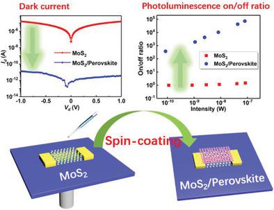
Toward pursuing high‐performance photodetectors based on 2D transition metal dichalcogenides (TMDs) such as molybdenum disulfide (MoS2), it is desirable to reduce the high dark current and sluggish response time. Here, in multilayer MoS2‐based photodetectors, a 2D halide perovskite, (C6H5C2H4NH3)2PbI4 ((PEA)2PbI4), is introduced as a bifunctional material: both as electron reservoir to reduce free carriers and passivation agent to passivate defects. Surprisingly, dark current is suppressed by six orders of magnitude after coating a (PEA)2PbI4 thin layer onto pristine MoS2 photodetector, with the dark current decreased to 10−11 A. This huge reduction of dark current suggests an efficient interlayer charge transfer from MoS2 to (PEA)2PbI4, which is further verified by photoluminescence quenching phenomenon. It indicates that (PEA)2PbI4 serves as electron reservoir to reduce carrier density of MoS2, resulting in ultrahigh detectivity (1.06 × 10¹³ Jones). Moreover, the response speed is also accelerated by more than 100‐fold due to passivation by 2D perovskite. In addition, it is found that this type of photodetectors can further work at self‐power mode (with the bias of 0 V). Therefore, the strategy of applying 2D perovskite on the surface of TMDs provides a novel way to fabricate high‐performance photodetectors.
中文翻译:

通过2D卤化物钙钛矿作为电子储库的极低暗电流MoS2光电探测器
为了追求基于二维过渡金属二卤化金属(TMD)的高性能光电探测器,例如二硫化钼(MoS 2),希望降低高暗电流和响应速度缓慢。在此,在基于MoS 2的多层光电探测器中,将二维卤化钙钛矿(C 6 H 5 C 2 H 4 NH 3)2 PbI 4((PEA)2 PbI 4)引入为双功能材料:均作为电子库减少自由载流子和钝化剂以钝化缺陷。令人惊讶的是,涂覆(PEA)2后暗电流被抑制了六个数量级。在原始MoS 2光电探测器上的PbI 4薄层,暗电流降至10 -11A。这种暗电流的巨大减少表明从MoS 2到(PEA)2 PbI 4的有效层间电荷转移,这已通过光致发光进一步验证淬火现象。这表明(PEA)2 PbI 4用作电子存储区以降低MoS 2的载流子密度,从而导致超高检测率(1.06×10 13琼斯)。此外,由于2D钙钛矿的钝化,响应速度也提高了100倍以上。此外,发现这种类型的光电探测器可以在自供电模式(偏置为0 V)下进一步工作。因此,将2D钙钛矿应用于TMD表面的策略提供了一种制造高性能光电探测器的新颖方法。
更新日期:2020-03-20
中文翻译:
通过2D卤化物钙钛矿作为电子储库的极低暗电流MoS2光电探测器
为了追求基于二维过渡金属二卤化金属(TMD)的高性能光电探测器,例如二硫化钼(MoS 2),希望降低高暗电流和响应速度缓慢。在此,在基于MoS 2的多层光电探测器中,将二维卤化钙钛矿(C 6 H 5 C 2 H 4 NH 3)2 PbI 4((PEA)2 PbI 4)引入为双功能材料:均作为电子库减少自由载流子和钝化剂以钝化缺陷。令人惊讶的是,涂覆(PEA)2后暗电流被抑制了六个数量级。在原始MoS 2光电探测器上的PbI 4薄层,暗电流降至10 -11A。这种暗电流的巨大减少表明从MoS 2到(PEA)2 PbI 4的有效层间电荷转移,这已通过光致发光进一步验证淬火现象。这表明(PEA)2 PbI 4用作电子存储区以降低MoS 2的载流子密度,从而导致超高检测率(1.06×10 13琼斯)。此外,由于2D钙钛矿的钝化,响应速度也提高了100倍以上。此外,发现这种类型的光电探测器可以在自供电模式(偏置为0 V)下进一步工作。因此,将2D钙钛矿应用于TMD表面的策略提供了一种制造高性能光电探测器的新颖方法。


 京公网安备 11010802027423号