当前位置:
X-MOL 学术
›
ACS Appl. Mater. Interfaces
›
论文详情
Our official English website, www.x-mol.net, welcomes your feedback! (Note: you will need to create a separate account there.)
Area-Selective ALD of Ru on Nanometer-Scale Cu Lines through Dimerization of Amino-Functionalized Alkoxy Silane Passivation Films.
ACS Applied Materials & Interfaces ( IF 9.5 ) Pub Date : 2020-01-08 , DOI: 10.1021/acsami.9b14596 Ivan Zyulkov 1, 2 , Viraj Madhiwala 3 , Ekaterina Voronina 4 , Matthew Snelgrove 5 , Justin Bogan 5 , Robert O'Connor 5 , Stefan De Gendt 1, 2 , Silvia Armini 2
ACS Applied Materials & Interfaces ( IF 9.5 ) Pub Date : 2020-01-08 , DOI: 10.1021/acsami.9b14596 Ivan Zyulkov 1, 2 , Viraj Madhiwala 3 , Ekaterina Voronina 4 , Matthew Snelgrove 5 , Justin Bogan 5 , Robert O'Connor 5 , Stefan De Gendt 1, 2 , Silvia Armini 2
Affiliation
|
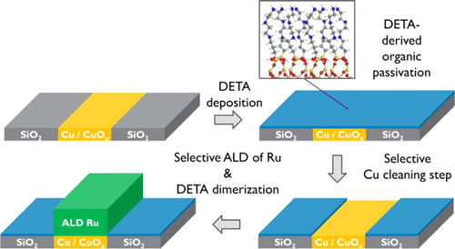
The selective deposition of materials on predefined areas on a substrate is of crucial importance for various applications, such as energy harvesting, microelectronic device fabrication, and catalysis. A representative example of area-confined deposition is the selective deposition of a metal film as the interconnect material in multilevel metallization schemes for CMOS technology. This allows the formation of multilevel structures with standard lithographical techniques while minimizing pattern misalignment and overlay and improving the uniformity of the structures across the wafer. In this work, area-selective deposition of Ru by atomic layer deposition (ALD) is investigated using alkoxy siloxane dielectric passivation layers. In this work, a comparison of several silane organic SAM precursors in terms of Ru ALD ASD performance is reported. The importance of the surface areal concentration of the passivation molecules is demonstrated. According to the in situ X-ray photoelectron spectroscopy film characterization, the ALD blocking layers derived from a (3-trimethoxysilylpropyl) diethylenetriamine (DETA) precursor have the ability to polymerize under ALD-compatible temperatures, such as 250 °C, which leads to a significant inhibition of Ru growth up to 400 ALD cycles. At the same time, the DETA layer can be selectively removed from the oxidized Cu surface by rinsing in acetic acid, which allows selective deposition of ca. 14 nm of Ru on Cu with no Ru detected on the DETA-coated surface by RBS. The approach is successfully tested on 50 nm half-pitch patterned SiO2/Cu lines.
中文翻译:

通过氨基官能化烷氧基硅烷钝化膜的二聚化,在纳米级Cu线上Ru的区域选择性ALD。
在基板的预定区域上选择性沉积材料对于各种应用(例如能量收集,微电子器件制造和催化)至关重要。区域限制沉积的一个代表性示例是在CMOS技术的多级金属化方案中选择性沉积金属膜作为互连材料。这允许用标准光刻技术形成多层结构,同时使图案未对准和覆盖最小化,并改善整个晶片上结构的均匀性。在这项工作中,研究了使用烷氧基硅氧烷介电钝化层通过原子层沉积(ALD)进行的区域选择性沉积Ru。在这项工作中,报告了几种硅烷有机SAM前体在Ru ALD ASD性能方面的比较。证明了钝化分子的表面面积浓度的重要性。根据原位X射线光电子能谱薄膜表征,衍生自(3-三甲氧基甲硅烷基丙基)二亚乙基三胺(DETA)前驱体的ALD阻挡层具有在ALD兼容温度(例如250°C)下聚合的能力,从而导致高达400个ALD循环对Ru的生长具有显着的抑制作用。同时,可以通过用乙酸冲洗从氧化的铜表面选择性地去除DETA层,从而选择性沉积ca。Cu上有14 nm的Ru,RBS在DETA涂层表面未检测到Ru。该方法已在50 nm半间距图案化SiO2 / Cu线上成功测试。根据原位X射线光电子能谱薄膜表征,衍生自(3-三甲氧基甲硅烷基丙基)二亚乙基三胺(DETA)前驱体的ALD阻挡层具有在ALD兼容温度(例如250°C)下聚合的能力,从而导致高达400个ALD循环对Ru的生长具有显着的抑制作用。同时,可以通过用乙酸冲洗从氧化的铜表面选择性地去除DETA层,从而选择性沉积ca。Cu上有14 nm的Ru,RBS在DETA涂层表面未检测到Ru。该方法已在50 nm半间距图案化SiO2 / Cu线上成功测试。根据原位X射线光电子能谱薄膜表征,衍生自(3-三甲氧基甲硅烷基丙基)二亚乙基三胺(DETA)前驱体的ALD阻挡层具有在ALD兼容温度(例如250°C)下聚合的能力,从而导致高达400个ALD循环对Ru的生长具有显着的抑制作用。同时,可以通过用乙酸冲洗从氧化的铜表面选择性地去除DETA层,从而选择性沉积ca。Cu上有14 nm的Ru,RBS在DETA涂层表面未检测到Ru。该方法已在50 nm半间距图案化SiO2 / Cu线上成功测试。衍生自(3-三甲氧基甲硅烷基丙基)二亚乙基三胺(DETA)前体的ALD阻隔层具有在ALD兼容温度(例如250°C)下聚合的能力,这导致Ru的生长受到抑制,直至400 ALD循环。同时,可以通过用乙酸冲洗从氧化的铜表面选择性地去除DETA层,从而选择性沉积ca。Cu上有14 nm的Ru,RBS在DETA涂层表面未检测到Ru。该方法已在50 nm半间距图案化SiO2 / Cu线上成功测试。衍生自(3-三甲氧基甲硅烷基丙基)二亚乙基三胺(DETA)前体的ALD阻隔层具有在ALD兼容温度(例如250°C)下聚合的能力,这导致Ru的生长受到抑制,直至400 ALD循环。同时,可以通过用乙酸冲洗从氧化的铜表面选择性地去除DETA层,从而选择性沉积ca。Cu上有14 nm的Ru,RBS在DETA涂层表面未检测到Ru。该方法已在50 nm半间距图案化SiO2 / Cu线上成功测试。Cu上有14 nm的Ru,RBS在DETA涂层表面未检测到Ru。该方法已在50 nm半间距图案化SiO2 / Cu线上成功测试。Cu上有14 nm的Ru,RBS在DETA涂层表面未检测到Ru。该方法已在50 nm半间距图案化SiO2 / Cu线上成功测试。
更新日期:2020-01-17
中文翻译:
通过氨基官能化烷氧基硅烷钝化膜的二聚化,在纳米级Cu线上Ru的区域选择性ALD。
在基板的预定区域上选择性沉积材料对于各种应用(例如能量收集,微电子器件制造和催化)至关重要。区域限制沉积的一个代表性示例是在CMOS技术的多级金属化方案中选择性沉积金属膜作为互连材料。这允许用标准光刻技术形成多层结构,同时使图案未对准和覆盖最小化,并改善整个晶片上结构的均匀性。在这项工作中,研究了使用烷氧基硅氧烷介电钝化层通过原子层沉积(ALD)进行的区域选择性沉积Ru。在这项工作中,报告了几种硅烷有机SAM前体在Ru ALD ASD性能方面的比较。证明了钝化分子的表面面积浓度的重要性。根据原位X射线光电子能谱薄膜表征,衍生自(3-三甲氧基甲硅烷基丙基)二亚乙基三胺(DETA)前驱体的ALD阻挡层具有在ALD兼容温度(例如250°C)下聚合的能力,从而导致高达400个ALD循环对Ru的生长具有显着的抑制作用。同时,可以通过用乙酸冲洗从氧化的铜表面选择性地去除DETA层,从而选择性沉积ca。Cu上有14 nm的Ru,RBS在DETA涂层表面未检测到Ru。该方法已在50 nm半间距图案化SiO2 / Cu线上成功测试。根据原位X射线光电子能谱薄膜表征,衍生自(3-三甲氧基甲硅烷基丙基)二亚乙基三胺(DETA)前驱体的ALD阻挡层具有在ALD兼容温度(例如250°C)下聚合的能力,从而导致高达400个ALD循环对Ru的生长具有显着的抑制作用。同时,可以通过用乙酸冲洗从氧化的铜表面选择性地去除DETA层,从而选择性沉积ca。Cu上有14 nm的Ru,RBS在DETA涂层表面未检测到Ru。该方法已在50 nm半间距图案化SiO2 / Cu线上成功测试。根据原位X射线光电子能谱薄膜表征,衍生自(3-三甲氧基甲硅烷基丙基)二亚乙基三胺(DETA)前驱体的ALD阻挡层具有在ALD兼容温度(例如250°C)下聚合的能力,从而导致高达400个ALD循环对Ru的生长具有显着的抑制作用。同时,可以通过用乙酸冲洗从氧化的铜表面选择性地去除DETA层,从而选择性沉积ca。Cu上有14 nm的Ru,RBS在DETA涂层表面未检测到Ru。该方法已在50 nm半间距图案化SiO2 / Cu线上成功测试。衍生自(3-三甲氧基甲硅烷基丙基)二亚乙基三胺(DETA)前体的ALD阻隔层具有在ALD兼容温度(例如250°C)下聚合的能力,这导致Ru的生长受到抑制,直至400 ALD循环。同时,可以通过用乙酸冲洗从氧化的铜表面选择性地去除DETA层,从而选择性沉积ca。Cu上有14 nm的Ru,RBS在DETA涂层表面未检测到Ru。该方法已在50 nm半间距图案化SiO2 / Cu线上成功测试。衍生自(3-三甲氧基甲硅烷基丙基)二亚乙基三胺(DETA)前体的ALD阻隔层具有在ALD兼容温度(例如250°C)下聚合的能力,这导致Ru的生长受到抑制,直至400 ALD循环。同时,可以通过用乙酸冲洗从氧化的铜表面选择性地去除DETA层,从而选择性沉积ca。Cu上有14 nm的Ru,RBS在DETA涂层表面未检测到Ru。该方法已在50 nm半间距图案化SiO2 / Cu线上成功测试。Cu上有14 nm的Ru,RBS在DETA涂层表面未检测到Ru。该方法已在50 nm半间距图案化SiO2 / Cu线上成功测试。Cu上有14 nm的Ru,RBS在DETA涂层表面未检测到Ru。该方法已在50 nm半间距图案化SiO2 / Cu线上成功测试。


 京公网安备 11010802027423号