Our official English website, www.x-mol.net, welcomes your
feedback! (Note: you will need to create a separate account there.)
Graphene-Transition Metal Dichalcogenide Heterojunctions for Scalable and Low-Power Complementary Integrated Circuits.
ACS Nano ( IF 15.8 ) Pub Date : 2020-01-06 , DOI: 10.1021/acsnano.9b08288 Chao-Hui Yeh,Zheng-Yong Liang,Yung-Chang Lin,Hsiang-Chieh Chen,Ta Fan,Chun-Hao Ma,Ying-Hao Chu,Kazu Suenaga,Po-Wen Chiu
ACS Nano ( IF 15.8 ) Pub Date : 2020-01-06 , DOI: 10.1021/acsnano.9b08288 Chao-Hui Yeh,Zheng-Yong Liang,Yung-Chang Lin,Hsiang-Chieh Chen,Ta Fan,Chun-Hao Ma,Ying-Hao Chu,Kazu Suenaga,Po-Wen Chiu
|
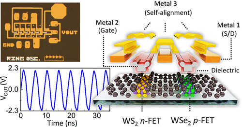
The most pressing barrier for the development of advanced electronics based on two-dimensional (2D) layered semiconductors stems from the lack of site-selective synthesis of complementary n- and p-channels with low contact resistance. Here, we report an in-plane epitaxial route for the growth of interlaced 2D semiconductor monolayers using chemical vapor deposition with a gas-confined scheme, in which patterned graphene (Gr) serves as a guiding template for site-selective growth of Gr-WS2-Gr and Gr-WSe2-Gr heterostructures. The Gr/2D semiconductor interface exhibits a transparent contact with a nearly ideal pinning factor of 0.95 for the n-channel WS2 and 0.92 for the p-channel WSe2. The effective depinning of the Fermi level gives an ultralow contact resistance of 0.75 and 1.20 kΩ·μm for WS2 and WSe2, respectively. Integrated logic circuits including inverter, NAND gate, static random access memory, and five-stage ring oscillator are constructed using the complementary Gr-WS2-Gr-WSe2-Gr heterojunctions as a fundamental building block, featuring the prominent performance metrics of high operation frequency (>0.2 GHz), low-power consumption, large noise margins, and high operational stability. The technology presented here provides a speculative look at the electronic circuitry built on atomic-scale semiconductors in the near future.
中文翻译:

用于可扩展和低功率互补集成电路的石墨烯过渡金属双硫族化物异质结。
基于二维(2D)分层半导体的先进电子学发展的最紧迫障碍是由于缺乏具有低接触电阻的互补n沟道和p沟道的位点选择性合成的缺乏。在这里,我们报告了一种采用气体限制方案的化学气相沉积法,用于隔行扫描二维半导体单层生长的面内外延路线,其中图案化石墨烯(Gr)用作Gr-WS2的位点选择性生长的指导模板-Gr和Gr-WSe2-Gr异质结构。Gr / 2D半导体界面呈现出透明的接触,n沟道WS2的理想钉扎系数为0.95,p沟道WSe2的理想钉扎系数为0.92。对于WS2和WSe2,费米能级的有效钉扎分别提供了0.75和1.20kΩ·μm的超低接触电阻。使用互补的Gr-WS2-Gr-WSe2-Gr异质结作为基本构件,构建了包括反相器,NAND门,静态随机存取存储器和五级环形振荡器的集成逻辑电路,其主要特征是高工作频率(> 0.2 GHz),低功耗,较大的噪声容限和较高的运行稳定性。本文介绍的技术可以在不久的将来对基于原子级半导体的电子电路进行推测。以及较高的运行稳定性。本文介绍的技术可以在不久的将来对基于原子级半导体的电子电路进行推测。以及较高的运行稳定性。本文介绍的技术可以在不久的将来对基于原子级半导体的电子电路进行推测。
更新日期:2020-01-09
中文翻译:
用于可扩展和低功率互补集成电路的石墨烯过渡金属双硫族化物异质结。
基于二维(2D)分层半导体的先进电子学发展的最紧迫障碍是由于缺乏具有低接触电阻的互补n沟道和p沟道的位点选择性合成的缺乏。在这里,我们报告了一种采用气体限制方案的化学气相沉积法,用于隔行扫描二维半导体单层生长的面内外延路线,其中图案化石墨烯(Gr)用作Gr-WS2的位点选择性生长的指导模板-Gr和Gr-WSe2-Gr异质结构。Gr / 2D半导体界面呈现出透明的接触,n沟道WS2的理想钉扎系数为0.95,p沟道WSe2的理想钉扎系数为0.92。对于WS2和WSe2,费米能级的有效钉扎分别提供了0.75和1.20kΩ·μm的超低接触电阻。使用互补的Gr-WS2-Gr-WSe2-Gr异质结作为基本构件,构建了包括反相器,NAND门,静态随机存取存储器和五级环形振荡器的集成逻辑电路,其主要特征是高工作频率(> 0.2 GHz),低功耗,较大的噪声容限和较高的运行稳定性。本文介绍的技术可以在不久的将来对基于原子级半导体的电子电路进行推测。以及较高的运行稳定性。本文介绍的技术可以在不久的将来对基于原子级半导体的电子电路进行推测。以及较高的运行稳定性。本文介绍的技术可以在不久的将来对基于原子级半导体的电子电路进行推测。


 京公网安备 11010802027423号