当前位置:
X-MOL 学术
›
ACS Appl. Electron. Mater.
›
论文详情
Our official English website, www.x-mol.net, welcomes your
feedback! (Note: you will need to create a separate account there.)
Hybrid Integration of n-MoS2/p-GaN Diodes by Quasi-van der Waals Epitaxy
ACS Applied Electronic Materials ( IF 4.3 ) Pub Date : 2020-01-23 , DOI: 10.1021/acsaelm.9b00607 Che-yu Liu, Hsien-chih Huang, Wonsik Choi, Jeongdong Kim, Kyooho Jung, Wei Sun, Nelson Tansu, Weidong Zhou, Hao-chung Kuo, Xiuling Li
ACS Applied Electronic Materials ( IF 4.3 ) Pub Date : 2020-01-23 , DOI: 10.1021/acsaelm.9b00607 Che-yu Liu, Hsien-chih Huang, Wonsik Choi, Jeongdong Kim, Kyooho Jung, Wei Sun, Nelson Tansu, Weidong Zhou, Hao-chung Kuo, Xiuling Li
|
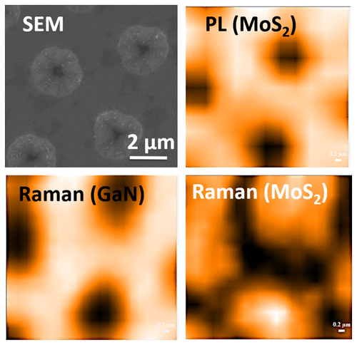
Compound semiconductor heterojunctions have enabled various optoelectronic devices. Nonetheless, the formation of heterojunctions is limited by the lattice matching between the two materials. On the other hand, two-dimensional (2D) semiconducting material and three-dimensional (3D) material heterojunction has attracted tremendous attention in recent years due to its immunity to the lattice mismatch. However, 2D/3D heterojunction formation by transferring 2D material suffers from contamination and defects created during the transfer process. Thus, direct growth of 2D material on 3D semiconducting material is crucial for the next generation heterojunction devices. In this work, we demonstrate n-MoS2/p-GaN diodes monolithically formed by quasi-van der Waals epitaxy. Monolayer MoS2 has been grown on a GaN substrate through a powder-based chemical vapor deposition (CVD) system. The triangular MoS2 flakes show well-aligned morphology with the GaN hexagonal crystal structure in the initial stage of the growth. Raman and PL mapping confirms the excellent uniformity of the monolayer MoS2 film on the GaN substrate. The growth of MoS2 on patterned GaN substrates are also studied, which yields monolayer and few-layer MoS2 formation on the planar surface and the pyramidal sidewalls, respectively. Finally, the n-MoS2/p-GaN diodes have been electrically characterized and show well-defined rectifying behavior with an ideality factor of ∼1.3.
中文翻译:

准范德华外延技术对n-MoS 2 / p-GaN二极管的混合集成
复合半导体异质结已使各种光电器件成为可能。但是,异质结的形成受到两种材料之间晶格匹配的限制。另一方面,二维(2D)半导体材料和三维(3D)材料异质结由于其对晶格失配的免疫力而近年来引起了极大的关注。但是,通过转移2D材料形成的2D / 3D异质结会受到污染,并在转移过程中产生缺陷。因此,在3D半导体材料上直接生长2D材料对于下一代异质结器件至关重要。在这项工作中,我们演示了由准范德华外延单片形成的n-MoS 2 / p-GaN二极管。单层MoS 2通过基于粉末的化学气相沉积(CVD)系统在氮化镓(GaN)衬底上生长氮化镓。在生长的初始阶段,三角形的MoS 2薄片显示出与GaN六角形晶体结构良好对齐的形态。拉曼和PL映射证实了GaN衬底上单层MoS 2膜的出色均匀性。还研究了MoS 2在图案化GaN衬底上的生长,该生长分别在平坦表面和金字塔形侧壁上形成单层和少层MoS 2。最后,对n-MoS 2 / p-GaN二极管进行了电学表征,并显示出明确的整流特性,理想因子约为1.3。
更新日期:2020-01-23
中文翻译:
准范德华外延技术对n-MoS 2 / p-GaN二极管的混合集成
复合半导体异质结已使各种光电器件成为可能。但是,异质结的形成受到两种材料之间晶格匹配的限制。另一方面,二维(2D)半导体材料和三维(3D)材料异质结由于其对晶格失配的免疫力而近年来引起了极大的关注。但是,通过转移2D材料形成的2D / 3D异质结会受到污染,并在转移过程中产生缺陷。因此,在3D半导体材料上直接生长2D材料对于下一代异质结器件至关重要。在这项工作中,我们演示了由准范德华外延单片形成的n-MoS 2 / p-GaN二极管。单层MoS 2通过基于粉末的化学气相沉积(CVD)系统在氮化镓(GaN)衬底上生长氮化镓。在生长的初始阶段,三角形的MoS 2薄片显示出与GaN六角形晶体结构良好对齐的形态。拉曼和PL映射证实了GaN衬底上单层MoS 2膜的出色均匀性。还研究了MoS 2在图案化GaN衬底上的生长,该生长分别在平坦表面和金字塔形侧壁上形成单层和少层MoS 2。最后,对n-MoS 2 / p-GaN二极管进行了电学表征,并显示出明确的整流特性,理想因子约为1.3。


 京公网安备 11010802027423号