当前位置:
X-MOL 学术
›
ACS Appl. Electron. Mater.
›
论文详情
Our official English website, www.x-mol.net, welcomes your feedback! (Note: you will need to create a separate account there.)
Effect of Copper Grain Size on the Interfacial Microstructure of a Sn/Cu Joint
ACS Applied Electronic Materials ( IF 4.7 ) Pub Date : 2020-01-13 , DOI: 10.1021/acsaelm.9b00720 Po-Fan Chan, Hsuan Lee, Shih-I Wen, Mao-Chun Hung, Chih-Ming Chen, Wei-Ping Dow
ACS Applied Electronic Materials ( IF 4.7 ) Pub Date : 2020-01-13 , DOI: 10.1021/acsaelm.9b00720 Po-Fan Chan, Hsuan Lee, Shih-I Wen, Mao-Chun Hung, Chih-Ming Chen, Wei-Ping Dow
|
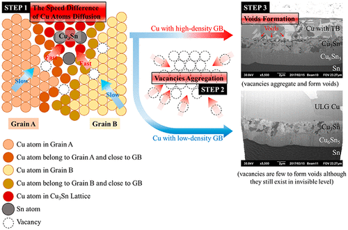
For pursuing a more comprehensive mechanism of void formation at the Sn/Cu interface, different grain size Cu samples with and without twinned boundaries are electrodeposited for the Sn/Cu joint and the IMC analysis. The formation of voids in the Sn/Cu joint is divided into three parts for discussion: Cu diffusion, Sn diffusion, and impurity diffusion. For the void formation at the Cu/Cu3Sn interface, the concept of the mechanism is from the Kirkendall effect, which is specially focused on the speed difference of Cu diffusion between at the Cu grain boundary and in the copper lattice in this study. The speed difference caused the vacancy formation. Impurities also play an important role in promoting the vacancy aggregation from a cluster to a void. Whether it is a diffusion effect or an impurity effect, it occurs at a Cu grain boundary. The voids would be formed when the density of the Cu grain boundary is high. The grain size of Cu is inversely proportional to the density of the Cu grain boundary; as a result, Cu grain size strongly affects the interfacial microstructure of a Sn/Cu joint, that is, the larger the Cu grain size is, the less the void at the Sn/Cu interface will be formed.
中文翻译:

铜晶粒尺寸对Sn / Cu接头界面微观结构的影响
为了追求更全面的在Sn / Cu界面形成空隙的机制,对具有和没有孪生边界的不同晶粒度的Cu样品进行电沉积,以进行Sn / Cu接头和IMC分析。Sn / Cu接头中形成的空隙分为三个部分进行讨论:Cu扩散,Sn扩散和杂质扩散。对于在Cu / Cu 3处形成空隙Sn界面,其机理的概念来自Kirkendall效应,在此研究中,该界面特别关注于Cu晶界和铜晶格之间的Cu扩散速度差。速度差异导致空缺的形成。杂质在促进空位聚集从簇到空的过程中也起着重要作用。无论是扩散效应还是杂质效应,它都会在Cu晶界发生。当Cu晶界的密度高时将形成空隙。Cu的晶粒尺寸与Cu晶界的密度成反比。结果,Cu粒径严重影响Sn / Cu接头的界面微观结构,即,Cu粒径越大,在Sn / Cu界面处形成的空隙越少。
更新日期:2020-01-13
中文翻译:
铜晶粒尺寸对Sn / Cu接头界面微观结构的影响
为了追求更全面的在Sn / Cu界面形成空隙的机制,对具有和没有孪生边界的不同晶粒度的Cu样品进行电沉积,以进行Sn / Cu接头和IMC分析。Sn / Cu接头中形成的空隙分为三个部分进行讨论:Cu扩散,Sn扩散和杂质扩散。对于在Cu / Cu 3处形成空隙Sn界面,其机理的概念来自Kirkendall效应,在此研究中,该界面特别关注于Cu晶界和铜晶格之间的Cu扩散速度差。速度差异导致空缺的形成。杂质在促进空位聚集从簇到空的过程中也起着重要作用。无论是扩散效应还是杂质效应,它都会在Cu晶界发生。当Cu晶界的密度高时将形成空隙。Cu的晶粒尺寸与Cu晶界的密度成反比。结果,Cu粒径严重影响Sn / Cu接头的界面微观结构,即,Cu粒径越大,在Sn / Cu界面处形成的空隙越少。


 京公网安备 11010802027423号