当前位置:
X-MOL 学术
›
ACS Appl. Electron. Mater.
›
论文详情
Our official English website, www.x-mol.net, welcomes your
feedback! (Note: you will need to create a separate account there.)
Application of Fluorescent Molecules as Noninvasive Sensors for Optoelectronic Characterization on Nanometer Length Scales
ACS Applied Electronic Materials ( IF 4.3 ) Pub Date : 2020-01-14 , DOI: 10.1021/acsaelm.9b00687 Thomas Ferschke 1 , Alexander Hofmann 2 , Wolfgang Brütting 2 , Jens Pflaum 1, 3
ACS Applied Electronic Materials ( IF 4.3 ) Pub Date : 2020-01-14 , DOI: 10.1021/acsaelm.9b00687 Thomas Ferschke 1 , Alexander Hofmann 2 , Wolfgang Brütting 2 , Jens Pflaum 1, 3
Affiliation
|
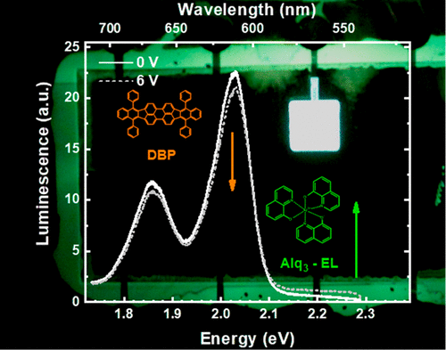
Determining noninvasively the microscopic optoelectronic parameters of molecular assemblies would constitute an important achievement in material as well as in life sciences. In this contribution, we cope with this challenge by utilizing fluorescent tetraphenyldibenzoperiflanthene (DBP) molecules as optically addressable sensors deterministically positioned in N,N′-di(1-naphthyl)-N,N′-diphenyl-(1,1′-biphenyl)-4,4′-diamine/tris(8-hydroxyquinolato)aluminum (NPB/Alq3) organic light-emitting diodes (OLEDs) as a model system. Measuring in operando the variation of the fluorescence intensity allows for direct correlation with the respective charge carrier distribution and transport processes at spatial resolutions below 15 nm as confirmed by complementary drift-diffusion simulations. Moreover, the molecular sensing technique renders sensitive enough to detect the presence of mobile charge carriers already below the built-in voltage. Operating the OLEDs under reverse bias, the sensing molecules provide information about the internal interface polarization caused by the alignment of the dipolar Alq3 entities during sample preparation. Benchmarking the macroscopic device behavior by means of electrical impedance measurements confirms the accuracy and reliability of the microscopic data obtained by the molecular sensing approach. Furthermore, the comparison demonstrates the dynamic range of the optical sensors being susceptible to variations in the local charge carrier distribution over several orders of magnitude and to interfacial polarization occurring at molecular heterojunctions within the OLED matrix. By its universality the presented sensing concept is applicable to a variety of molecular systems and, thus, being of relevance not only for OLEDs but also for other organic thin film devices like transistors.
中文翻译:

荧光分子在纳米长度尺度上用于光电特性的无创传感器的应用
非侵入性地确定分子组装体的微观光电参数将在材料以及生命科学中构成重要的成就。在这项贡献中,我们通过利用荧光四苯基二苯并过环蒽(DBP)分子作为光学可寻址传感器确定地位于N,N'-二(1-萘基)-N,N'-二苯基-(1,1'-联苯)中来应对这一挑战)-4,4'-二胺/三(8-羟基喹啉基)铝(NPB / Alq 3)有机发光二极管(OLED)作为模型系统。测量在operando荧光强度的变化允许与低于15 nm的空间分辨率下的相应电荷载流子分布和传输过程直接相关,这已通过互补漂移扩散模拟得到了证实。此外,分子感测技术的灵敏度足以检测已经低于内置电压的移动载流子。在反向偏置下操作OLED,传感分子可提供有关由偶极Alq 3的排列引起的内部界面极化的信息样品制备过程中的实体。通过电阻抗测量对宏观设备行为进行基准测试,可以确认通过分子传感方法获得的微观数据的准确性和可靠性。此外,该比较表明,光学传感器的动态范围容易受到局部电荷载流子分布在几个数量级上的变化的影响,并且易于发生在OLED矩阵内的分子异质结处的界面偏振。通过其普遍性,提出的感测概念可应用于各种分子系统,因此,不仅与OLED相关,而且与其他有机薄膜器件(如晶体管)相关。
更新日期:2020-01-14
中文翻译:
荧光分子在纳米长度尺度上用于光电特性的无创传感器的应用
非侵入性地确定分子组装体的微观光电参数将在材料以及生命科学中构成重要的成就。在这项贡献中,我们通过利用荧光四苯基二苯并过环蒽(DBP)分子作为光学可寻址传感器确定地位于N,N'-二(1-萘基)-N,N'-二苯基-(1,1'-联苯)中来应对这一挑战)-4,4'-二胺/三(8-羟基喹啉基)铝(NPB / Alq 3)有机发光二极管(OLED)作为模型系统。测量在operando荧光强度的变化允许与低于15 nm的空间分辨率下的相应电荷载流子分布和传输过程直接相关,这已通过互补漂移扩散模拟得到了证实。此外,分子感测技术的灵敏度足以检测已经低于内置电压的移动载流子。在反向偏置下操作OLED,传感分子可提供有关由偶极Alq 3的排列引起的内部界面极化的信息样品制备过程中的实体。通过电阻抗测量对宏观设备行为进行基准测试,可以确认通过分子传感方法获得的微观数据的准确性和可靠性。此外,该比较表明,光学传感器的动态范围容易受到局部电荷载流子分布在几个数量级上的变化的影响,并且易于发生在OLED矩阵内的分子异质结处的界面偏振。通过其普遍性,提出的感测概念可应用于各种分子系统,因此,不仅与OLED相关,而且与其他有机薄膜器件(如晶体管)相关。


 京公网安备 11010802027423号