当前位置:
X-MOL 学术
›
ACS Appl. Electron. Mater.
›
论文详情
Our official English website, www.x-mol.net, welcomes your
feedback! (Note: you will need to create a separate account there.)
Sn-Doped CdS Nanowires with Low-Temperature Lasing by CW-Laser Excitation
ACS Applied Electronic Materials ( IF 4.3 ) Pub Date : 2020-01-14 , DOI: 10.1021/acsaelm.9b00766 Li Zhang 1 , Ruibin Liu 1 , Bingsuo Zou 1, 2
ACS Applied Electronic Materials ( IF 4.3 ) Pub Date : 2020-01-14 , DOI: 10.1021/acsaelm.9b00766 Li Zhang 1 , Ruibin Liu 1 , Bingsuo Zou 1, 2
Affiliation
|
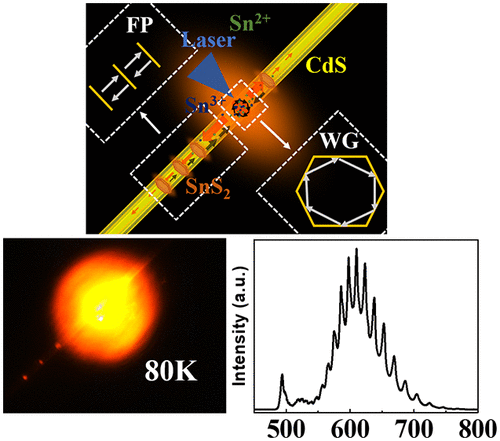
Sn-doped CdS nanowires, with the inside coexisting Sn(II)S, Sn2(III)S3, and Sn(IV)S2 identified by in situ Raman and XPS spectra, are grown via a simple thermal evaporation deposition technique. Its room-temperature photoluminescence (PL) spectrum shows a broad in-gap emission band out of different Sn dopants which is also superposed by a series of weak modes from a microcavity due to the wire size and its structure, besides the CdS band-edge emission and a side-band emission due to SnS2. The ratio of the intensity of the in-gap emission versus that of the band-edge emission is only 1/4 at room temperature, but it can be remarkably increased to about 7 at 80 K. This significant enhancement of the in-gap emission may be attributed to the local plasma coming from more bound carriers and enhanced microcavity effect at low temperature by analyzing the temperature-dependent PL and Raman spectra in detail. For these reasons, the band-edge and in-gap emission both can realize lasing excited by a continuous laser at 80 K. The results would provide a way to get temperature tunable low threshold microscale lasers and study the plasma-polariton process within a microcavity.
中文翻译:

连续激光激发低温低温掺锡的CdS纳米线
通过简单的热蒸发沉积技术生长内部掺有Sn(II)S,Sn 2(III)S 3和Sn(IV)S 2的掺Sn的CdS纳米线。它的室温光致发光(PL)光谱显示出来自不同Sn掺杂剂的宽的能隙内发射带,除了CdS带边缘外,由于线径和其结构,它还由于微腔而被一系列微腔的弱模叠加SnS 2引起的发射和边带发射。在室温下,带隙内发射的强度与带状边沿发射的强度之比仅为1/4,但在80 K时可以显着增加到约7。间隙内发射的这种显着增强通过详细分析温度相关的PL和拉曼光谱,可以归因于来自更多结合载流子的局部等离子体和低温下增强的微腔效应。由于这些原因,带边沿和带隙内发射都可以实现由80 K的连续激光激发的激光。结果将提供一种获得温度可调的低阈值微尺度激光并研究微腔内的等离子体极化过程的方法。 。
更新日期:2020-01-15
中文翻译:
连续激光激发低温低温掺锡的CdS纳米线
通过简单的热蒸发沉积技术生长内部掺有Sn(II)S,Sn 2(III)S 3和Sn(IV)S 2的掺Sn的CdS纳米线。它的室温光致发光(PL)光谱显示出来自不同Sn掺杂剂的宽的能隙内发射带,除了CdS带边缘外,由于线径和其结构,它还由于微腔而被一系列微腔的弱模叠加SnS 2引起的发射和边带发射。在室温下,带隙内发射的强度与带状边沿发射的强度之比仅为1/4,但在80 K时可以显着增加到约7。间隙内发射的这种显着增强通过详细分析温度相关的PL和拉曼光谱,可以归因于来自更多结合载流子的局部等离子体和低温下增强的微腔效应。由于这些原因,带边沿和带隙内发射都可以实现由80 K的连续激光激发的激光。结果将提供一种获得温度可调的低阈值微尺度激光并研究微腔内的等离子体极化过程的方法。 。


 京公网安备 11010802027423号