当前位置:
X-MOL 学术
›
ACS Appl. Electron. Mater.
›
论文详情
Our official English website, www.x-mol.net, welcomes your
feedback! (Note: you will need to create a separate account there.)
Transparent and Conductive Molybdenum-Doped ZnO Thin Films via Chemical Vapor Deposition
ACS Applied Electronic Materials ( IF 4.3 ) Pub Date : 2020-01-14 , DOI: 10.1021/acsaelm.9b00647 Donglei Zhao 1 , Sanjayan Sathasivam 1 , Jianwei Li 1 , Claire J. Carmalt 1
ACS Applied Electronic Materials ( IF 4.3 ) Pub Date : 2020-01-14 , DOI: 10.1021/acsaelm.9b00647 Donglei Zhao 1 , Sanjayan Sathasivam 1 , Jianwei Li 1 , Claire J. Carmalt 1
Affiliation
|
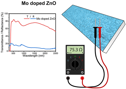
Extrinsically doped ZnO is widely used as a transparent conducting electrode and has the potential to alleviate the demand on the expensive but ubiquitous Sn-doped In2O3. Here, we report for the first time the synthesis and characterization of molybdenum-doped ZnO via a chemical vapor deposition route. Films were grown by using diethylzinc, molybdenum hexacarbonyl, toluene, and methanol. All films had visible light transmittance of ∼80% and electrical resistivity of 10–3 Ω·cm with the lowest resistivity of 2.6 × 10⁻³ Ω·cm observed for the 0.57 at. % Mo-doped film. X-ray photoelectron spectroscopy of the surface species and X-ray diffraction based calculations of the ZnO unit cell parameters suggest that Mo is present in the 4+ oxidation state, thus contributing two electrons for electrical conduction for every Zn2+ ion replaced in the lattice.
中文翻译:

通过化学气相沉积的透明导电钼掺杂的ZnO薄膜
外在掺杂的ZnO被广泛用作透明导电电极,并且具有减轻对昂贵但普遍存在的Sn掺杂的In 2 O 3的需求的潜力。在这里,我们首次通过化学气相沉积途径报道了掺钼的ZnO的合成和表征。通过使用二乙基锌,六羰基钼,甲苯和甲醇来生长膜。所有膜具有〜80%的可见光透射率和10的电阻率-3 Ω·cm的具有2.6×10的电阻率最低-3Ω·cm为0.57 at。钼掺杂薄膜。表面物种的X射线光电子能谱和基于ZnO晶胞参数的X射线衍射计算表明,Mo以4+氧化态存在,因此,对于在ZnO中被取代的每个Zn 2+离子,都有两个电子用于导电。格子。
更新日期:2020-01-15
中文翻译:
通过化学气相沉积的透明导电钼掺杂的ZnO薄膜
外在掺杂的ZnO被广泛用作透明导电电极,并且具有减轻对昂贵但普遍存在的Sn掺杂的In 2 O 3的需求的潜力。在这里,我们首次通过化学气相沉积途径报道了掺钼的ZnO的合成和表征。通过使用二乙基锌,六羰基钼,甲苯和甲醇来生长膜。所有膜具有〜80%的可见光透射率和10的电阻率-3 Ω·cm的具有2.6×10的电阻率最低-3Ω·cm为0.57 at。钼掺杂薄膜。表面物种的X射线光电子能谱和基于ZnO晶胞参数的X射线衍射计算表明,Mo以4+氧化态存在,因此,对于在ZnO中被取代的每个Zn 2+离子,都有两个电子用于导电。格子。


 京公网安备 11010802027423号