当前位置:
X-MOL 学术
›
ACS Appl. Electron. Mater.
›
论文详情
Our official English website, www.x-mol.net, welcomes your
feedback! (Note: you will need to create a separate account there.)
Submicrometer Resolution Hyperspectral Quantum Rod Thermal Imaging of Microelectronic Devices
ACS Applied Electronic Materials ( IF 4.3 ) Pub Date : 2020-01-15 , DOI: 10.1021/acsaelm.9b00575 Bahar Öner 1 , James W. Pomeroy 1 , Martin Kuball 1
ACS Applied Electronic Materials ( IF 4.3 ) Pub Date : 2020-01-15 , DOI: 10.1021/acsaelm.9b00575 Bahar Öner 1 , James W. Pomeroy 1 , Martin Kuball 1
Affiliation
|
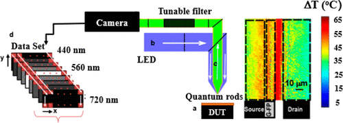
The trend of electronic device miniaturization, from the microscale to the nanoscale, presents a temperature measurement challenge. The available techniques have limitations in terms of either resolution, calibration, acquisition time, or equipment cost. Here we demonstrate a thermography technique called hyperspectral quantum rod thermal imaging (HQTI), which exploits temperature-dependent photoluminescence (PL) emission of quantum rods to obtain the surface temperature map of a biased electronic device, with a straightforward calibration. This method uses relatively simple, low-cost equipment, while achieving submicrometer spatial resolution. This technique is demonstrated by measuring the thermal map of a direct current (dc) operated gallium nitride (GaN) high electron mobility transistor (HEMT), achieving a temperature precision of ∼4 °C and an ∼700–800 nm estimated lateral optical resolution. This is a versatile method for measurement both in submicrometer scale regions of interest and of larger areas in the hundreds of micrometers range.
中文翻译:

亚微米分辨率的高光谱微电子器件量子棒热成像
从微米级到纳米级的电子设备小型化趋势提出了温度测量的挑战。可用的技术在分辨率,校准,采集时间或设备成本方面都有局限性。在这里,我们演示了一种称为高光谱量子棒热成像(HQTI)的热成像技术,该技术利用量子棒的温度依赖性光致发光(PL)发射来获得带有偏置的电子设备的表面温度图,并进行简单的校准。该方法使用相对简单,低成本的设备,同时实现了亚微米的空间分辨率。通过测量直流(dc)操作的氮化镓(GaN)高电子迁移率晶体管(HEMT)的热图来证明该技术,达到约4°C的温度精度和约700–800 nm的估计横向光学分辨率。这是一种用于在感兴趣的亚微米级范围内和数百微米范围内的较大区域进行测量的通用方法。
更新日期:2020-01-15
中文翻译:
亚微米分辨率的高光谱微电子器件量子棒热成像
从微米级到纳米级的电子设备小型化趋势提出了温度测量的挑战。可用的技术在分辨率,校准,采集时间或设备成本方面都有局限性。在这里,我们演示了一种称为高光谱量子棒热成像(HQTI)的热成像技术,该技术利用量子棒的温度依赖性光致发光(PL)发射来获得带有偏置的电子设备的表面温度图,并进行简单的校准。该方法使用相对简单,低成本的设备,同时实现了亚微米的空间分辨率。通过测量直流(dc)操作的氮化镓(GaN)高电子迁移率晶体管(HEMT)的热图来证明该技术,达到约4°C的温度精度和约700–800 nm的估计横向光学分辨率。这是一种用于在感兴趣的亚微米级范围内和数百微米范围内的较大区域进行测量的通用方法。


 京公网安备 11010802027423号