当前位置:
X-MOL 学术
›
Phys. Rev. X
›
论文详情
Our official English website, www.x-mol.net, welcomes your
feedback! (Note: you will need to create a separate account there.)
Spectroscopic Visualization of a Robust Electronic Response of Semiconducting Nanowires to Deposition of Superconducting Islands
Physical Review X ( IF 11.6 ) Pub Date : 2020-01-03 , DOI: 10.1103/physrevx.10.011002 Jonathan Reiner , Abhay Kumar Nayak , Amit Tulchinsky , Aviram Steinbok , Tom Koren , Noam Morali , Rajib Batabyal , Jung-Hyun Kang , Nurit Avraham , Yuval Oreg , Hadas Shtrikman , Haim Beidenkopf
Physical Review X ( IF 11.6 ) Pub Date : 2020-01-03 , DOI: 10.1103/physrevx.10.011002 Jonathan Reiner , Abhay Kumar Nayak , Amit Tulchinsky , Aviram Steinbok , Tom Koren , Noam Morali , Rajib Batabyal , Jung-Hyun Kang , Nurit Avraham , Yuval Oreg , Hadas Shtrikman , Haim Beidenkopf
|
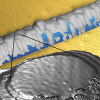
Following significant progress in the visualization and characterization of Majorana end modes in hybrid systems of semiconducting nanowires and superconducting islands, much attention is devoted to the investigation of the electronic structure at the buried interface between the semiconductor and the superconductor. The properties of that interface and the structure of the electronic wave functions that occupy it determine the functionality and the topological nature of the superconducting state induced therein. Here we study this buried interface by performing spectroscopic mappings of superconducting aluminum islands epitaxially grown in situ on indium arsenide nanowires. We find unexpected robustness of the hybrid system as the direct contact with the aluminum islands does not lead to any change in the chemical potential of the nanowires, nor does it induce a significant band bending in their vicinity. We attribute this to the presence of surface states bound to the facets of the nanowire. Such surface states, which are present also in bare nanowires prior to aluminum deposition, pin the Fermi level, thus rendering the nanowires resilient to surface perturbations. The aluminum islands further display Coulomb blockade gaps and peaks that signify the formation of a resistive tunneling barrier at the InAs-Al interface. The extracted interface resistivity, , will allow us to proximity induce superconductivity with negligible Coulomb blockade effects by islands with interface area as small as . At low energies we identify a potential energy barrier that further suppresses the transmittance through the interface. A corresponding barrier exists in bare semiconductors between surface states and the accumulation layer, induced to maintain charge neutrality. Our observations elucidate the delicate interplay between the resistive nature of the InAs-Al interface and the ability to proximitize superconductivity and tune the chemical potential in semiconductor-superconductor hybrid nanowires.
中文翻译:

半导体纳米线对超导岛沉积的鲁棒电子响应的光谱可视化
在半导体纳米线和超导岛的混合系统中Majorana端模的可视化和表征方面取得了重大进展之后,半导体和超导体之间掩埋界面的电子结构研究得到了极大的关注。该界面的性质和占据该界面的电子波函数的结构决定了其中感应的超导状态的功能和拓扑性质。在这里,我们通过对原位外延生长的超导铝岛进行光谱映射来研究该埋藏界面在砷化铟纳米线上。我们发现混合系统具有出乎意料的坚固性,因为与铝岛的直接接触不会导致纳米线的化学势发生任何变化,也不会在纳米线附近引起明显的能带弯曲。我们将其归因于与纳米线的小面结合的表面状态的存在。在铝沉积之前裸露的纳米线中也存在这种表面状态,使费米能级固定,从而使纳米线对表面扰动具有弹性。铝岛还显示出库仑阻挡间隙和峰,这表明在InAs-Al界面处形成了电阻隧穿势垒。提取的界面电阻率,将使我们能够通过界面面积小至的小岛接近感应超导,并具有可忽略的库仑阻塞效应 。在低能量下,我们确定了一个势垒,该势垒进一步抑制了通过界面的透射率。在表面状态和累积层之间的裸露半导体中存在相应的势垒,被诱导以保持电荷中性。我们的观察阐明了InAs-Al界面的电阻性质与代理超导性和调节半导体-超导体混合纳米线中化学势的能力之间的微妙相互作用。
更新日期:2020-01-04
中文翻译:
半导体纳米线对超导岛沉积的鲁棒电子响应的光谱可视化
在半导体纳米线和超导岛的混合系统中Majorana端模的可视化和表征方面取得了重大进展之后,半导体和超导体之间掩埋界面的电子结构研究得到了极大的关注。该界面的性质和占据该界面的电子波函数的结构决定了其中感应的超导状态的功能和拓扑性质。在这里,我们通过对原位外延生长的超导铝岛进行光谱映射来研究该埋藏界面在砷化铟纳米线上。我们发现混合系统具有出乎意料的坚固性,因为与铝岛的直接接触不会导致纳米线的化学势发生任何变化,也不会在纳米线附近引起明显的能带弯曲。我们将其归因于与纳米线的小面结合的表面状态的存在。在铝沉积之前裸露的纳米线中也存在这种表面状态,使费米能级固定,从而使纳米线对表面扰动具有弹性。铝岛还显示出库仑阻挡间隙和峰,这表明在InAs-Al界面处形成了电阻隧穿势垒。提取的界面电阻率,将使我们能够通过界面面积小至的小岛接近感应超导,并具有可忽略的库仑阻塞效应 。在低能量下,我们确定了一个势垒,该势垒进一步抑制了通过界面的透射率。在表面状态和累积层之间的裸露半导体中存在相应的势垒,被诱导以保持电荷中性。我们的观察阐明了InAs-Al界面的电阻性质与代理超导性和调节半导体-超导体混合纳米线中化学势的能力之间的微妙相互作用。


 京公网安备 11010802027423号