当前位置:
X-MOL 学术
›
ACS Appl. Nano Mater.
›
论文详情
Our official English website, www.x-mol.net, welcomes your
feedback! (Note: you will need to create a separate account there.)
In-Situ Transmission Electron Microscopy Imaging of Aluminum Diffusion in Germanium Nanowires for the Fabrication of Sub-10 nm Ge Quantum Disks
ACS Applied Nano Materials ( IF 5.3 ) Pub Date : 2020-01-16 , DOI: 10.1021/acsanm.9b02564 M.A. Luong 1 , E. Robin 1 , N. Pauc 2 , P. Gentile 2 , M. Sistani 3 , A. Lugstein 3 , M. Spies 4 , B. Fernandez 4 , M. I. Den Hertog 4
ACS Applied Nano Materials ( IF 5.3 ) Pub Date : 2020-01-16 , DOI: 10.1021/acsanm.9b02564 M.A. Luong 1 , E. Robin 1 , N. Pauc 2 , P. Gentile 2 , M. Sistani 3 , A. Lugstein 3 , M. Spies 4 , B. Fernandez 4 , M. I. Den Hertog 4
Affiliation
|
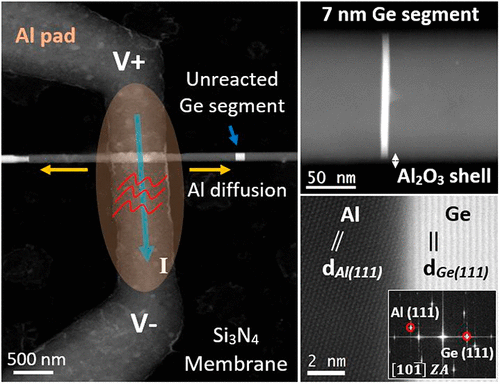
The thermal activated solid state reaction forming aluminum–germanium nanowire (NW) heterostructures is a promising system as very sharp and well-defined one-dimensional contacts can be created between a metal and a semiconductor, that can become a quantum dot if the size becomes sufficiently small. In the search for high performance devices without variability, it is of high interest to allow deterministic fabrication of nanowire quantum dots, avoiding sample variability and obtaining atomic scale precision on the fabricated dot size. In this paper, we present a proof of principle experiment to produce sub-10 nm Ge quantum disks (QDs), using a combination of ex-situ thermal annealing via rapid thermal annealing (RTA) and in-situ Joule heating technique in a transmission electron microscope (TEM). First we present in-situ direct joule heating experiments showing how the heating electrode could be damaged due to the formation of Al crystals and voids at the vicinity of the metal/NW contact, likely related with electro-migration phenomena. We show that the contact quality can be preserved by including an additional ex-situ RTA step prior to the in-situ heating. The in-situ observations also show in real-time how the exchange reaction initiates simultaneously from several locations underneath the Al contact pad, and the Al crystal grows gradually inside the initial Ge NW with the growth interface along a Ge {111} lattice plane. Once the reaction front moves out from underneath the contact metal, two factors jeopardize an atomically accurate control of the Al/Ge reaction interface. We observed a local acceleration of the reaction interface due to the electron beam irradiation in the transmission electron microscope as well as the appearance of large jumps of the interface in unpassivated Ge wires, whereas a smooth advancement of the reaction interface was observed in wires with an Al2O3 passivation shell on the surface. Carefully controlling all aspects of the exchange reaction, we demonstrate a proof of principle experiment combining ex-situ and in-situ heating techniques to precisely control and produce axial Al/Ge/Al NW heterostructures with an ultrashort Ge segment down to 7 nm. Practically, the scaling down of the Ge segment length is only limited by the microscope resolution.
中文翻译:

锗纳米线中铝扩散用于亚10 nm Ge量子盘制造的原位透射电子显微镜成像
形成铝-锗纳米线(NW)异质结构的热活化固态反应是一种很有前途的系统,因为可以在金属和半导体之间建立非常清晰且定义明确的一维接触,如果尺寸变大,则可以变成量子点。足够小。在寻找无变异性的高性能器件时,非常重要的是允许确定性地制造纳米线量子点,避免样品的变异性并获得所制造的点尺寸的原子尺度精度。在本文中,我们提出了原理性实验的证明,该技术结合了通过快速热退火(RTA)进行的非原位热退火和传输中的原地焦耳加热技术来生产10 nm以下的Ge量子盘(QD)电子显微镜(TEM)。首先,我们提出了原位直接焦耳加热实验,该实验表明加热电极如何由于金属/ NW接触附近的Al晶体和空隙的形成而损坏,这可能与电迁移现象有关。我们表明,可以通过在原位加热之前包括一个额外的异位RTA步骤来保持接触质量。原位观察还实时显示交换反应如何同时从Al接触垫下方的多个位置同时引发,Al晶体在初始Ge NW内逐渐生长,其生长界面沿Ge {111}晶格面。一旦反应前沿从接触金属下方移出,就会有两个因素危及Al / Ge反应界面的原子精确控制。表面有2 O 3钝化壳。仔细地控制交换反应的各个方面,我们证明了原理实验的证明,其结合了非原位和原位加热技术来精确控制和生产轴向Ge / Al / Al NW异质结构,Ge链段低至7 nm。实际上,锗段长度的缩小仅受显微镜分辨率的限制。
更新日期:2020-01-17
中文翻译:
锗纳米线中铝扩散用于亚10 nm Ge量子盘制造的原位透射电子显微镜成像
形成铝-锗纳米线(NW)异质结构的热活化固态反应是一种很有前途的系统,因为可以在金属和半导体之间建立非常清晰且定义明确的一维接触,如果尺寸变大,则可以变成量子点。足够小。在寻找无变异性的高性能器件时,非常重要的是允许确定性地制造纳米线量子点,避免样品的变异性并获得所制造的点尺寸的原子尺度精度。在本文中,我们提出了原理性实验的证明,该技术结合了通过快速热退火(RTA)进行的非原位热退火和传输中的原地焦耳加热技术来生产10 nm以下的Ge量子盘(QD)电子显微镜(TEM)。首先,我们提出了原位直接焦耳加热实验,该实验表明加热电极如何由于金属/ NW接触附近的Al晶体和空隙的形成而损坏,这可能与电迁移现象有关。我们表明,可以通过在原位加热之前包括一个额外的异位RTA步骤来保持接触质量。原位观察还实时显示交换反应如何同时从Al接触垫下方的多个位置同时引发,Al晶体在初始Ge NW内逐渐生长,其生长界面沿Ge {111}晶格面。一旦反应前沿从接触金属下方移出,就会有两个因素危及Al / Ge反应界面的原子精确控制。表面有2 O 3钝化壳。仔细地控制交换反应的各个方面,我们证明了原理实验的证明,其结合了非原位和原位加热技术来精确控制和生产轴向Ge / Al / Al NW异质结构,Ge链段低至7 nm。实际上,锗段长度的缩小仅受显微镜分辨率的限制。


 京公网安备 11010802027423号