Our official English website, www.x-mol.net, welcomes your
feedback! (Note: you will need to create a separate account there.)
Electric-field-tuned topological phase transition in ultrathin Na3Bi
Nature ( IF 50.5 ) Pub Date : 2018-12-01 , DOI: 10.1038/s41586-018-0788-5 James L. Collins , Anton Tadich , Weikang Wu , Lidia C. Gomes , Joao N. B. Rodrigues , Chang Liu , Jack Hellerstedt , Hyejin Ryu , Shujie Tang , Sung-Kwan Mo , Shaffique Adam , Shengyuan A. Yang , Michael S. Fuhrer , Mark T. Edmonds
Nature ( IF 50.5 ) Pub Date : 2018-12-01 , DOI: 10.1038/s41586-018-0788-5 James L. Collins , Anton Tadich , Weikang Wu , Lidia C. Gomes , Joao N. B. Rodrigues , Chang Liu , Jack Hellerstedt , Hyejin Ryu , Shujie Tang , Sung-Kwan Mo , Shaffique Adam , Shengyuan A. Yang , Michael S. Fuhrer , Mark T. Edmonds
|
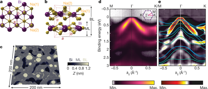
The electric field induced quantum phase transition from topological to conventional insulator has been proposed as the basis of a topological field effect transistor [1-4]. In this scheme an electric field can switch ‘on’ the ballistic flow of charge and spin along dissipationless edges of the two-dimensional (2D) quantum spin Hall insulator [5-9], and when ‘off’ is a conventional insulator with no conductive channels. Such a topological transistor is promising for low-energy logic circuits [4], which would necessitate electric field-switched materials with conventional and topological bandgaps much greater than room temperature, significantly greater than proposed to date [6-8]. Topological Dirac semimetals (TDS) are promising systems in which to look for topological field-effect switching, as they lie at the boundary between conventional and topological phases [3,10-16]. Here we use scanning probe microscopy/spectroscopy (STM/STS) and angle-resolved photoelectron spectroscopy (ARPES) to show that monoand bilayer films of TDS Na3Bi [3,17] are 2D topological insulators with bulk bandgaps >400 meV in the absence of electric field. Upon application of electric field by doping with potassium or by close approach of the STM tip, the bandgap can be completely closed then re-opened with conventional gap greater than 100 meV. The large bandgaps in both the conventional and quantum spin Hall phases, much greater than the thermal energy kT = 25 meV at room temperature, suggest that ultrathin Na3Bi is suitable for room temperature topological transistor operation. Two-dimensional Quantum Spin Hall (QSH) insulators are characterized by an insulating interior with bulk bandgap Eg, and topologically protected conducting edge channels that are robust to backscattering by non-magnetic disorder. The QSH effect was first realized in HgTe quantum wells [5] where the small Eg prevents device applications above cryogenic temperatures. This has led to efforts to find new materials with Eg >> 25 meV (thermal energy at room temperature) for room temperature topological electronic devices. Recent reports of QSH insulators bismuthene on SiC (Eg ~ 0.8 eV) [6] and monolayer 1T′-WTe2 (Eg ~ 50 meV) [7] are promising, with the quantum spin Hall effect measured in monolayer WTe2 up to 100K [8,9]. However, a predicted electric-field effect in WTe2 has not yet been reported, and a substantial field-effect in atomically two-dimensional bismuthene is unlikely due to the completely in-plane structure that lacks inversion symmetry meaning any Stark effect would most likely be small. Ultrathin films of topological Dirac semimetals (TDS) are a promising material class to realise the electric-field tuned topological phase transition, with such a transition predicted in few-layer films of TDS Na3Bi and Cd3As2 [3]. Bulk TDSs are zero-bandgap semimetals with a linear band dispersion in all three dimensions around pairs of Dirac points [10-13], whilst few-layer TDSs are predicted to be non-trivial insulators with bulk bandgaps up to ~300 meV for monolayer Na3Bi [17]. However, experiments on few-layer TDSs are presently lacking [14-16]. To unambiguously demonstrate electric field control over the magnitude, electric field-dependence, and topological nature of the bandgap in ultrathin Na3Bi, we employ two independent experimental techniques. First, we utilize ARPES to directly measure the electronic bandstructure and its modification as a result of doping the surface with potassium to generate an electric field. Second, we use scanning tunnelling spectroscopy (STS), which measures the local density of states (DOS) as a function of energy, to directly probe the energy gap while varying the tip-sample separation and consequently the induced electric field caused by the potential difference between tip and sample. STS also resolves the topological edge state in Na3Bi at low electric field, demonstrating the topological nature of this phase. The unit cell of Na3Bi contains two stacked triple layers in the z direction, comprising Na and Bi atoms that form a honeycomb lattice, with interleaved Na atoms as shown in the crystal structures of Fig. 1(a)(b). One triple layer and two stacked triple layers correspond to monolayer (ML) and bilayer (BL) Na3Bi respectively as illustrated in Fig. 1(b). Figure 1(c) shows the Brillouin zone of 2D Na3Bi. In Fig. 1(d) STM on few-layer Na3Bi(001) epitaxial films grown via molecular beam epitaxy (MBE) on Si(111) (see methods and SM1 for details) reveals coexisting regions of ML and BL Na3Bi islands that are atomically flat and up to 40 nm in size, along with small areas of bare substrate. Monolayer regions are identified by an additional 0.22 nm distance to the underlying substrate, due to interfacial spacing or structural relaxation which has been observed previously in other atomically thin materials [18]. Figure 1(e) shows the overall band structure of few-layer Na3Bi films along the M -K surface directions measured with ARPES at hv = 48 eV. Figure 1(f) shows the second derivative of the spectra in order to enhance low intensity features. This has been overlaid with density functional theory (DFT) calculations for ML (blue) and BL (green) Na3Bi showing good agreement, consistent with the STM topography which shows coexisting ML and BL regions. Photon-energy dependent ARPES (see SM2) demonstrates that the film is electronically 2D, with no dispersion in kz unlike its bulk or 15 nm thin-film counterparts [10,15]. Depth dependent X-ray photoelectron spectroscopy (XPS) (See SM1), revealed no additional components observed in either the Si2p core level corresponding to the Si(111) substrate or the Na and Bi core levels of Na3Bi, verifying Na3Bi is free-standing on Si(111). We first measure the size of the bulk bandgap for ML and BL regions of Na3Bi by probing the electronic structure with STS, which measures the differential conductance dI/dV as a function of sample bias V, and is proportional to the local density of states. Figure 2(a) shows typical dI/dV spectra for ML (red) and BL (black) with bandgaps corresponding to 0.44 ± 0.01 eV and 0.41 ± 0.01 eV respectively (see SM3 for details on extracting bandgap values). All STS curves in Fig. 2(a) were taken more than 5 nm inwards from step edges. Figure 2(b) plots the experimental bandgap (blue squares) in comparison to DFT calculated values for pristine Na3Bi (black circles) and Na3Bi layers that contain an Na(2) surface vacancy (red circles) (see Methods for details, with associated bandstructures found in SM4). The ~0.15 eV discrepancy between experiment and DFT for ML is likely a result of the underestimation of electronic bandgap well known to occur in DFT calculations [19]. The minimal change in bandgap from ML to BL observed experimentally is well explained by the DFT calculations that include Na(2) surface vacancies; this vacancy gives rise to a delocalized resonance feature and enhancement of the electronic bandgap [20], resulting in only a small layer-dependent evolution in bandgap. To verify the prediction that ML and BL Na3Bi are large bandgap QSH insulators (see Fig. S4) we probe the step edge of these islands to the underlying Si(111) substrate to look for the conductive edge state signature of a QSH insulator (STM topography shown in Fig. 2(c)). Figure 2(d) shows local dI/dV spectra taken on BL Na3Bi far away from the edge (black curve) and at the edge (blue curve). In contrast to the gap in the bulk, the dI/dV at the edge is quite different, with states filling the bulk gap along with a characteristic dip at 0 mV bias. Similar features observed in other QSH insulators 1T’-WTe2 [7] and bismuthene [6] have been attributed to one-dimensional (1D) non-trivial edge states and the emergence of a Luttinger liquid [21]. Figure 2(e) probes dI/dV as a function of distance away from the edge, demonstrating the extended nature of the edge state feature, with Fig. 2(f) showing that the dI/dV signal within the bulk bandgap moving away from the edge follows the expected exponential decay for a 1D topological non-trivial state [6]. With ML and BL Na3Bi verified as large bandgap QSH insulators, we now examine the role of electric field on modifying the size and nature of the bandgap. First, we utilize ARPES to measure the bandstructure after doping the surface with K to generate an electric field. Details on calculating the displacement field are in SM5. Figure 3(a)-(d) shows the bandstructure along K for values of the electric field of 0.0, 0.72, 1.44 and 2.18 Vnm respectively, with the green and blue dots reflecting the extracted maxima from energy distribution curve (EDC) and momentum distribution curve (MDC) analysis (see SM5 for details). The right panel in (a)-(d) represents a model of a 2D gapped Dirac system (see SM5). In Fig. 3(a) only the hole band is observable, which away from displays a linear band dispersion (hole Fermi velocity of vF ~ 3x10 ms). The band dispersion near displays the clear cusp of a band edge indicating a gapped system, with 140 meV separation between the valence band edge and the Fermi energy EF. The effect of K dosing in Figs. 3(b)-(d) is to n-type dope the sample and consequently increase the displacement field. At a displacement field of 0.7 Vnm the separation from the valence band edge to EF has increased to ~257 meV. The bandgap must be at least this amount, consistent with STS, though we cannot determine its exact magnitude since the conduction band lies above EF (although it can be estimated see Fig. S7(a)). Upon increasing the displacement field, a Diraclike electron band emerges (electron Fermi velocity of vF ~ 10 ms). At 1.4 Vnm the extracted gap between the two band edges is ~100 meV, and reduces to ~90 meV at 2.2 Vnm (see Supplementary Materials S5 for calculation and comparison with STS values). Whilst a significant reduction in bandgap with displacement field occurs, due to the finite energy width of the bands (~100 meV) we c
中文翻译:

超薄 Na3Bi 中电场调谐的拓扑相变
从拓扑绝缘体到常规绝缘体的电场诱导量子相变已被提议作为拓扑场效应晶体管的基础 [1-4]。在这个方案中,电场可以“开启”电荷和自旋沿二维 (2D) 量子自旋霍尔绝缘体的无耗散边缘的弹道流动 [5-9],当“关闭”时,传统绝缘体没有导电通道。这种拓扑晶体管有希望用于低能量逻辑电路 [4],这将需要具有远大于室温的常规和拓扑带隙的电场开关材料,显着大于迄今为止提出的 [6-8]。拓扑狄拉克半金属 (TDS) 是寻找拓扑场效应开关的有前途的系统,因为它们位于常规相和拓扑相之间的边界 [3,10-16]。在这里,我们使用扫描探针显微镜/光谱 (STM/STS) 和角分辨光电子能谱 (ARPES) 来表明 TDS Na3Bi [3,17] 的单层和双层膜是二维拓扑绝缘体,在没有电场。在通过掺杂钾或靠近 STM 尖端施加电场后,带隙可以完全关闭,然后以大于 100 meV 的常规间隙重新打开。常规和量子自旋霍尔相中的大带隙,远大于室温下的热能 kT = 25 meV,表明超薄 Na3Bi 适用于室温拓扑晶体管操作。二维量子自旋霍尔 (QSH) 绝缘体的特点是具有体带隙 Eg 的绝缘内部和拓扑保护的导电边缘通道,这些通道对非磁性无序的反向散射具有鲁棒性。QSH 效应首先在 HgTe 量子阱 [5] 中实现,其中小的 Eg 阻止了高于低温的设备应用。这导致人们努力寻找用于室温拓扑电子设备的 Eg >> 25 meV(室温下的热能)的新材料。最近关于 SiC (Eg ~ 0.8 eV) [6] 和单层 1T'-WTe2 (Eg ~ 50 meV) [7] 上的 QSH 绝缘体铋的报告很有希望,在单层 WTe2 中测量的量子自旋霍尔效应高达 100K [8] ,9]。然而,尚未报道 WTe2 中预测的电场效应,由于完全面内结构缺乏反转对称性,这意味着任何斯塔克效应都很可能很小,因此原子二维铋中的大量场效应不太可能发生。拓扑狄拉克半金属 (TDS) 的超薄膜是实现电场调谐拓扑相变的有前途的材料类别,在 TDS Na3Bi 和 Cd3As2 的几层薄膜中预测了这种转变 [3]。体 TDS 是零带隙半金属,在围绕狄拉克点对 [10-13] 的所有三个维度上具有线性能带色散,而预计少层 TDS 是非平凡绝缘体,单层体带隙高达 ~300 meV Na3Bi [17]。然而,目前缺乏对少层 TDS 的实验 [14-16]。为了明确地证明电场对幅度的控制,超薄 Na3Bi 中带隙的电场依赖性和拓扑性质,我们采用了两种独立的实验技术。首先,我们利用 ARPES 直接测量电子能带结构及其在表面掺杂钾以产生电场的结果。其次,我们使用扫描隧道光谱 (STS),它测量局部态密度 (DOS) 作为能量的函数,在改变尖端样品分离的同时直接探测能隙,从而改变由电位引起的感应电场针尖和样品的区别。STS 还解决了低电场下 Na3Bi 的拓扑边缘状态,证明了该相的拓扑性质。Na3Bi 的晶胞在 z 方向包含两个堆叠的三层,包含形成蜂窝晶格的 Na 和 Bi 原子,具有交错的 Na 原子,如图 1(a)(b) 的晶体结构所示。一个三层和两个堆叠的三层分别对应于单层(ML)和双层(BL)Na3Bi,如图1(b)所示。图 1(c) 显示了二维 Na3Bi 的布里渊区。在图 1(d) 中,在 Si(111) 上通过分子束外延 (MBE) 生长的少层 Na3Bi(001) 外延膜上的 STM(详见方法和 SM1)揭示了 ML 和 BL Na3Bi 岛的共存区域原子级平坦,尺寸高达 40 nm,以及小面积的裸基板。由于界面间距或结构弛豫,之前在其他原子级薄材料中观察到了这种情况,因此单层区域通过与下方基板的额外 0.22 nm 距离来识别 [18]。图 1(e) 显示了沿 M -K 表面方向使用 ARPES 在 hv = 48 eV 下测量的少层 Na3Bi 薄膜的整体能带结构。图 1(f) 显示了光谱的二阶导数,以增强低强度特征。这已与 ML(蓝色)和 BL(绿色)Na3Bi 的密度泛函理论 (DFT) 计算重叠,显示出良好的一致性,与显示 ML 和 BL 区域共存的 STM 地形一致。与光子能量相关的 ARPES(参见 SM2)表明该薄膜是电子二维的,与其体膜或 15 nm 薄膜对应物不同,在 kz 中没有色散 [10,15]。深度相关的 X 射线光电子能谱 (XPS)(见 SM1)显示在对应于 Si(111)衬底的 Si2p 核心水平或 Na3Bi 的 Na 和 Bi 核心水平中没有观察到额外的成分,验证 Na3Bi 在 Si(111) 上是独立的。我们首先通过用 STS 探测电子结构来测量 Na3Bi ML 和 BL 区域的体带隙大小,STS 测量微分电导 dI/dV 作为样品偏置 V 的函数,并且与局部状态密度成正比。图 2(a) 显示了 ML(红色)和 BL(黑色)的典型 dI/dV 光谱,带隙分别对应于 0.44 ± 0.01 eV 和 0.41 ± 0.01 eV(有关提取带隙值的详细信息,请参见 SM3)。图 2(a)中的所有 STS 曲线都是从台阶边缘向内超过 5 nm 的。图 2(b) 绘制了实验带隙(蓝色方块)与原始 Na3Bi(黑色圆圈)和包含 Na(2) 表面空位(红色圆圈)的 Na3Bi 层的 DFT 计算值相比(详见方法,以及相关的在 SM4 中发现的能带结构)。〜0。ML 的实验和 DFT 之间的 15 eV 差异可能是由于 DFT 计算中众所周知的电子带隙被低估所致 [19]。实验观察到的从 ML 到 BL 的带隙的最小变化可以通过包括 Na(2) 表面空位的 DFT 计算得到很好的解释;这种空位引起了离域共振特征和电子带隙的增强 [20],导致带隙中只有一个小的依赖于层的演化。为了验证 ML 和 BL Na3Bi 是大带隙 QSH 绝缘体的预测(见图 S4),我们将这些岛的阶梯边缘探测到下面的 Si(111)衬底,以寻找 QSH 绝缘体(STM)的导电边缘状态特征地形如图2(c)所示)。图 2(d) 显示了在远离边缘(黑色曲线)和边缘(蓝色曲线)的 BL Na3Bi 上获取的局部 dI/dV 光谱。与体间隙相比,边缘处的 dI/dV 完全不同,状态填充体间隙以及在 0 mV 偏压下的特征下降。在其他 QSH 绝缘体 1T'-WTe2 [7] 和铋 [6] 中观察到的类似特征归因于一维 (1D) 非平凡边缘状态和 Luttinger 液体 [21] 的出现。图 2(e) 探测 dI/dV 作为距边缘距离的函数,展示了边缘状态特征的扩展性质,图 2(f) 显示体带隙内的 dI/dV 信号远离边缘边缘遵循一维拓扑非平凡状态的预期指数衰减 [6]。ML 和 BL Na3Bi 被验证为大带隙 QSH 绝缘体,我们现在检查电场在改变带隙大小和性质方面的作用。首先,我们利用 ARPES 在表面掺杂 K 以产生电场后测量能带结构。有关计算位移场的详细信息在 SM5 中。图 3(a)-(d) 分别显示了电场值为 0.0、0.72、1.44 和 2.18 Vnm 时沿 K 的能带结构,绿色和蓝色点反映了从能量分布曲线 (EDC) 和动量分布曲线 (MDC) 分析(详见 SM5)。(a)-(d) 中的右侧面板表示 2D 有隙狄拉克系统的模型(参见 SM5)。在图 3(a) 中,仅可观察到空穴带,远离 显示线性带色散(空穴费米速度为 vF ~ 3x10 ms)。 附近的能带色散显示了能带边缘的清晰尖端,表明有隙系统,价带边缘和费米能量 EF 之间的距离为 140 meV。图 1 中 K 剂量的影响 3(b)-(d) 是对样品进行 n 型掺杂,从而增加位移场。在 0.7 Vnm 的位移场下,从价带边缘到 EF 的距离增加到~257 meV。带隙必须至少是这个量,与 STS 一致,尽管我们无法确定它的确切大小,因为导带位于 EF 之上(尽管可以估计见图 S7(a))。随着位移场的增加,出现类似狄拉克的电子带(电子费米速度为 vF ~ 10 ms)。在 1.4 Vnm 时,两个带边缘之间的提取间隙为 ~100 meV,并在 2 时降低到 ~90 meV。2 Vnm(有关计算和与 STS 值的比较,请参阅补充材料 S5)。虽然随着位移场的带隙显着减小,但由于带的有限能量宽度(~100 meV),我们 c
更新日期:2018-12-01
中文翻译:
超薄 Na3Bi 中电场调谐的拓扑相变
从拓扑绝缘体到常规绝缘体的电场诱导量子相变已被提议作为拓扑场效应晶体管的基础 [1-4]。在这个方案中,电场可以“开启”电荷和自旋沿二维 (2D) 量子自旋霍尔绝缘体的无耗散边缘的弹道流动 [5-9],当“关闭”时,传统绝缘体没有导电通道。这种拓扑晶体管有希望用于低能量逻辑电路 [4],这将需要具有远大于室温的常规和拓扑带隙的电场开关材料,显着大于迄今为止提出的 [6-8]。拓扑狄拉克半金属 (TDS) 是寻找拓扑场效应开关的有前途的系统,因为它们位于常规相和拓扑相之间的边界 [3,10-16]。在这里,我们使用扫描探针显微镜/光谱 (STM/STS) 和角分辨光电子能谱 (ARPES) 来表明 TDS Na3Bi [3,17] 的单层和双层膜是二维拓扑绝缘体,在没有电场。在通过掺杂钾或靠近 STM 尖端施加电场后,带隙可以完全关闭,然后以大于 100 meV 的常规间隙重新打开。常规和量子自旋霍尔相中的大带隙,远大于室温下的热能 kT = 25 meV,表明超薄 Na3Bi 适用于室温拓扑晶体管操作。二维量子自旋霍尔 (QSH) 绝缘体的特点是具有体带隙 Eg 的绝缘内部和拓扑保护的导电边缘通道,这些通道对非磁性无序的反向散射具有鲁棒性。QSH 效应首先在 HgTe 量子阱 [5] 中实现,其中小的 Eg 阻止了高于低温的设备应用。这导致人们努力寻找用于室温拓扑电子设备的 Eg >> 25 meV(室温下的热能)的新材料。最近关于 SiC (Eg ~ 0.8 eV) [6] 和单层 1T'-WTe2 (Eg ~ 50 meV) [7] 上的 QSH 绝缘体铋的报告很有希望,在单层 WTe2 中测量的量子自旋霍尔效应高达 100K [8] ,9]。然而,尚未报道 WTe2 中预测的电场效应,由于完全面内结构缺乏反转对称性,这意味着任何斯塔克效应都很可能很小,因此原子二维铋中的大量场效应不太可能发生。拓扑狄拉克半金属 (TDS) 的超薄膜是实现电场调谐拓扑相变的有前途的材料类别,在 TDS Na3Bi 和 Cd3As2 的几层薄膜中预测了这种转变 [3]。体 TDS 是零带隙半金属,在围绕狄拉克点对 [10-13] 的所有三个维度上具有线性能带色散,而预计少层 TDS 是非平凡绝缘体,单层体带隙高达 ~300 meV Na3Bi [17]。然而,目前缺乏对少层 TDS 的实验 [14-16]。为了明确地证明电场对幅度的控制,超薄 Na3Bi 中带隙的电场依赖性和拓扑性质,我们采用了两种独立的实验技术。首先,我们利用 ARPES 直接测量电子能带结构及其在表面掺杂钾以产生电场的结果。其次,我们使用扫描隧道光谱 (STS),它测量局部态密度 (DOS) 作为能量的函数,在改变尖端样品分离的同时直接探测能隙,从而改变由电位引起的感应电场针尖和样品的区别。STS 还解决了低电场下 Na3Bi 的拓扑边缘状态,证明了该相的拓扑性质。Na3Bi 的晶胞在 z 方向包含两个堆叠的三层,包含形成蜂窝晶格的 Na 和 Bi 原子,具有交错的 Na 原子,如图 1(a)(b) 的晶体结构所示。一个三层和两个堆叠的三层分别对应于单层(ML)和双层(BL)Na3Bi,如图1(b)所示。图 1(c) 显示了二维 Na3Bi 的布里渊区。在图 1(d) 中,在 Si(111) 上通过分子束外延 (MBE) 生长的少层 Na3Bi(001) 外延膜上的 STM(详见方法和 SM1)揭示了 ML 和 BL Na3Bi 岛的共存区域原子级平坦,尺寸高达 40 nm,以及小面积的裸基板。由于界面间距或结构弛豫,之前在其他原子级薄材料中观察到了这种情况,因此单层区域通过与下方基板的额外 0.22 nm 距离来识别 [18]。图 1(e) 显示了沿 M -K 表面方向使用 ARPES 在 hv = 48 eV 下测量的少层 Na3Bi 薄膜的整体能带结构。图 1(f) 显示了光谱的二阶导数,以增强低强度特征。这已与 ML(蓝色)和 BL(绿色)Na3Bi 的密度泛函理论 (DFT) 计算重叠,显示出良好的一致性,与显示 ML 和 BL 区域共存的 STM 地形一致。与光子能量相关的 ARPES(参见 SM2)表明该薄膜是电子二维的,与其体膜或 15 nm 薄膜对应物不同,在 kz 中没有色散 [10,15]。深度相关的 X 射线光电子能谱 (XPS)(见 SM1)显示在对应于 Si(111)衬底的 Si2p 核心水平或 Na3Bi 的 Na 和 Bi 核心水平中没有观察到额外的成分,验证 Na3Bi 在 Si(111) 上是独立的。我们首先通过用 STS 探测电子结构来测量 Na3Bi ML 和 BL 区域的体带隙大小,STS 测量微分电导 dI/dV 作为样品偏置 V 的函数,并且与局部状态密度成正比。图 2(a) 显示了 ML(红色)和 BL(黑色)的典型 dI/dV 光谱,带隙分别对应于 0.44 ± 0.01 eV 和 0.41 ± 0.01 eV(有关提取带隙值的详细信息,请参见 SM3)。图 2(a)中的所有 STS 曲线都是从台阶边缘向内超过 5 nm 的。图 2(b) 绘制了实验带隙(蓝色方块)与原始 Na3Bi(黑色圆圈)和包含 Na(2) 表面空位(红色圆圈)的 Na3Bi 层的 DFT 计算值相比(详见方法,以及相关的在 SM4 中发现的能带结构)。〜0。ML 的实验和 DFT 之间的 15 eV 差异可能是由于 DFT 计算中众所周知的电子带隙被低估所致 [19]。实验观察到的从 ML 到 BL 的带隙的最小变化可以通过包括 Na(2) 表面空位的 DFT 计算得到很好的解释;这种空位引起了离域共振特征和电子带隙的增强 [20],导致带隙中只有一个小的依赖于层的演化。为了验证 ML 和 BL Na3Bi 是大带隙 QSH 绝缘体的预测(见图 S4),我们将这些岛的阶梯边缘探测到下面的 Si(111)衬底,以寻找 QSH 绝缘体(STM)的导电边缘状态特征地形如图2(c)所示)。图 2(d) 显示了在远离边缘(黑色曲线)和边缘(蓝色曲线)的 BL Na3Bi 上获取的局部 dI/dV 光谱。与体间隙相比,边缘处的 dI/dV 完全不同,状态填充体间隙以及在 0 mV 偏压下的特征下降。在其他 QSH 绝缘体 1T'-WTe2 [7] 和铋 [6] 中观察到的类似特征归因于一维 (1D) 非平凡边缘状态和 Luttinger 液体 [21] 的出现。图 2(e) 探测 dI/dV 作为距边缘距离的函数,展示了边缘状态特征的扩展性质,图 2(f) 显示体带隙内的 dI/dV 信号远离边缘边缘遵循一维拓扑非平凡状态的预期指数衰减 [6]。ML 和 BL Na3Bi 被验证为大带隙 QSH 绝缘体,我们现在检查电场在改变带隙大小和性质方面的作用。首先,我们利用 ARPES 在表面掺杂 K 以产生电场后测量能带结构。有关计算位移场的详细信息在 SM5 中。图 3(a)-(d) 分别显示了电场值为 0.0、0.72、1.44 和 2.18 Vnm 时沿 K 的能带结构,绿色和蓝色点反映了从能量分布曲线 (EDC) 和动量分布曲线 (MDC) 分析(详见 SM5)。(a)-(d) 中的右侧面板表示 2D 有隙狄拉克系统的模型(参见 SM5)。在图 3(a) 中,仅可观察到空穴带,远离 显示线性带色散(空穴费米速度为 vF ~ 3x10 ms)。 附近的能带色散显示了能带边缘的清晰尖端,表明有隙系统,价带边缘和费米能量 EF 之间的距离为 140 meV。图 1 中 K 剂量的影响 3(b)-(d) 是对样品进行 n 型掺杂,从而增加位移场。在 0.7 Vnm 的位移场下,从价带边缘到 EF 的距离增加到~257 meV。带隙必须至少是这个量,与 STS 一致,尽管我们无法确定它的确切大小,因为导带位于 EF 之上(尽管可以估计见图 S7(a))。随着位移场的增加,出现类似狄拉克的电子带(电子费米速度为 vF ~ 10 ms)。在 1.4 Vnm 时,两个带边缘之间的提取间隙为 ~100 meV,并在 2 时降低到 ~90 meV。2 Vnm(有关计算和与 STS 值的比较,请参阅补充材料 S5)。虽然随着位移场的带隙显着减小,但由于带的有限能量宽度(~100 meV),我们 c


 京公网安备 11010802027423号