当前位置:
X-MOL 学术
›
Acc. Chem. Res.
›
论文详情
Our official English website, www.x-mol.net, welcomes your
feedback! (Note: you will need to create a separate account there.)
Emerging Design and Characterization Guidelines for Polymer-Based Infrared Photodetectors
Accounts of Chemical Research ( IF 16.4 ) Pub Date : 2018-12-06 00:00:00 , DOI: 10.1021/acs.accounts.8b00446 Zhenghui Wu 1 , Yichen Zhai 1 , Hyonwoong Kim 1 , Jason D. Azoulay 2 , Tse Nga Ng 1
Accounts of Chemical Research ( IF 16.4 ) Pub Date : 2018-12-06 00:00:00 , DOI: 10.1021/acs.accounts.8b00446 Zhenghui Wu 1 , Yichen Zhai 1 , Hyonwoong Kim 1 , Jason D. Azoulay 2 , Tse Nga Ng 1
Affiliation
|
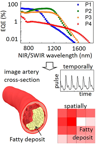
Infrared photodetectors are essential to many applications, including surveillance, communications, process monitoring, and biological imaging. The short-wave infrared (SWIR) spectral region (λ = 1–3 μm) is particularly powerful for health monitoring and medical diagnostics because biological tissues show low absorbance and minimal SWIR autofluorescence, enabling greater penetration depth and improved resolution in comparison with visible light. However, current SWIR photodetection technologies are largely based on epitaxially grown inorganic semiconductors, which are costly, require complex processing, and impose cooling requirements incompatible with wearable electronics. Solution-processable semiconductors are being developed for infrared detectors to enable low-cost direct deposition and facilitate monolithic integration and resolution not achievable using current technologies. In particular, organic semiconductors offer numerous advantages, including large-area and conformal coverage, temperature insensitivity, and biocompatibility, for enabling ubiquitous SWIR optoelectronics.
中文翻译:

基于聚合物的红外光电探测器的新兴设计和表征指南
红外光电探测器对于许多应用都是必不可少的,包括监视,通信,过程监控和生物成像。短波红外(SWIR)光谱区域(λ= 1-3μm)对健康监测和医学诊断特别有效,因为生物组织显示出低吸收性和最小的SWIR自发荧光,与可见光相比,具有更大的穿透深度和更高的分辨率。但是,当前的SWIR光电检测技术主要基于外延生长的无机半导体,这很昂贵,需要复杂的处理过程,并且提出了与可穿戴电子设备不兼容的冷却要求。正在开发用于红外探测器的可溶液处理的半导体,以实现低成本的直接沉积,并促进单片集成和使用现有技术无法实现的分辨率。尤其是,有机半导体具有众多优势,包括大面积和保形覆盖,温度不敏感性和生物相容性,可实现无处不在的SWIR光电。
更新日期:2018-12-06
中文翻译:
基于聚合物的红外光电探测器的新兴设计和表征指南
红外光电探测器对于许多应用都是必不可少的,包括监视,通信,过程监控和生物成像。短波红外(SWIR)光谱区域(λ= 1-3μm)对健康监测和医学诊断特别有效,因为生物组织显示出低吸收性和最小的SWIR自发荧光,与可见光相比,具有更大的穿透深度和更高的分辨率。但是,当前的SWIR光电检测技术主要基于外延生长的无机半导体,这很昂贵,需要复杂的处理过程,并且提出了与可穿戴电子设备不兼容的冷却要求。正在开发用于红外探测器的可溶液处理的半导体,以实现低成本的直接沉积,并促进单片集成和使用现有技术无法实现的分辨率。尤其是,有机半导体具有众多优势,包括大面积和保形覆盖,温度不敏感性和生物相容性,可实现无处不在的SWIR光电。


 京公网安备 11010802027423号