Our official English website, www.x-mol.net, welcomes your
feedback! (Note: you will need to create a separate account there.)
Charge-Transport Mechanisms in CuInSexS2–x Quantum-Dot Films
ACS Nano ( IF 15.8 ) Pub Date : 2018-11-29 00:00:00 , DOI: 10.1021/acsnano.8b07179 Hyeong Jin Yun 1 , Jaehoon Lim 1, 2 , Addis S. Fuhr 1, 3 , Nikolay S. Makarov 1, 4 , Sam Keene 5 , Matt Law 5 , Jeffrey M. Pietryga 1 , Victor I. Klimov 1
ACS Nano ( IF 15.8 ) Pub Date : 2018-11-29 00:00:00 , DOI: 10.1021/acsnano.8b07179 Hyeong Jin Yun 1 , Jaehoon Lim 1, 2 , Addis S. Fuhr 1, 3 , Nikolay S. Makarov 1, 4 , Sam Keene 5 , Matt Law 5 , Jeffrey M. Pietryga 1 , Victor I. Klimov 1
Affiliation
|
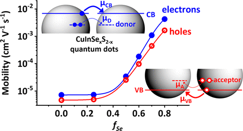
Colloidal quantum dots (QDs) have attracted considerable attention as promising materials for solution-processable electronic and optoelectronic devices. Copper indium selenium sulfide (CuInSexS2–x or CISeS) QDs are particularly attractive as an environmentally benign alternative to the much more extensively studied QDs containing toxic metals such as Cd and Pb. Carrier transport properties of CISeS-QD films, however, are still poorly understood. Here, we aim to elucidate the factors that control charge conductance in CISeS QD solids and, based on this knowledge, develop practical approaches for controlling the polarity of charge transport and carrier mobilities. To this end, we incorporate CISeS QDs into field-effect transistors (FETs) and perform detailed characterization of these devices as a function of the Se/(Se+S) ratio, surface treatment, thermal annealing, and the identity of source and drain electrodes. We observe that as-synthesized CuInSexS2–x QDs exhibit degenerate p-type transport, likely due to metal vacancies and CuIn’’ anti-site defects (Cu1+ on an In3+ site) that act as acceptor states. Moderate-temperature annealing of the films in the presence of indium source and drain electrodes leads to switching of the transport polarity to nondegenerate n-type, which can be attributed to the formation of In-related defects such as InCu•• (an In3+ cation on a Cu1+ site) or Ini••• (interstitial In3+) acting as donors. We observe that the carrier mobilities increase dramatically (by 3 orders of magnitude) with increasing Se/(Se+S) ratio in both n- and p-type devices. To explain this observation, we propose a two-state conductance model, which invokes a high-mobility intrinsic band-edge state and a low-mobility defect-related intragap state. These states are thermally coupled, and their relative occupancies depend on both QD composition and temperature. Our observations suggest that the increase in the relative fraction of Se moves conduction- and valence band edges closer to low-mobility intragap levels. This results in increased relative occupancy of the intrinsic band-edge states and a corresponding growth of the measured mobility. Further improvement in charge-transport characteristics of the CISeS QD samples as well as their stability is obtained by infilling the QD films with amorphous Al2O3 using atomic layer deposition.
中文翻译:

CuInSe x S 2– x量子点薄膜中的电荷传输机制
胶体量子点(QD)作为可溶液加工的电子和光电设备的有前途的材料吸引了相当多的关注。硫化铜铟硒(CuInSe x S 2– xQDs作为一种对环境无害的替代品,尤其是对环境有益的替代品,因为它是对Cd和Pb等有毒金属进行更广泛研究的QD的替代品。但是,对CISeS-QD薄膜的载流子传输特性仍然知之甚少。在这里,我们旨在阐明控制CISeS QD固体中电荷电导的因素,并基于此知识,开发控制电荷传输和载流子迁移极性的实用方法。为此,我们将CISeS QD集成到场效应晶体管(FET)中,并根据Se /(Se + S)比,表面处理,热退火以及源极和漏极的特性对这些器件进行详细的表征电极。我们观察到合成后的CuInSe x S 2– x量子点显示出简并的p型传输,这可能是由于金属空位和充当受体态的Cu In ''反位缺陷(In 3+位上的Cu 1+)所致。在存在铟源电极和漏电极的情况下对膜进行适度的温度退火会导致传输极性转换为未简并的n型,这可归因于形成In相关的缺陷,例如In Cu ••(In 3+在Cu阳离子1+位点)或在我•••(间质性在3+)充当捐赠者。我们观察到,在n-和p处,随着Se /(Se + S)比的增加,载流子迁移率显着增加(3个数量级)。型设备。为了解释这一现象,我们提出了一种两种状态的电导模型,该模型调用了高迁移率的固有能带边缘状态和低迁移率的缺陷相关的能隙内部状态。这些状态是热耦合的,它们的相对占用率取决于QD成分和温度。我们的观察结果表明,硒相对含量的增加将导带和价带边缘移近低迁移率能隙内水平。这导致固有带边缘态的相对占有率增加,并且所测量的迁移率相应增加。通过使用原子层沉积用非晶态Al 2 O 3填充QD膜,可以进一步改善CISeS QD样品的电荷传输特性及其稳定性。
更新日期:2018-11-29
中文翻译:
CuInSe x S 2– x量子点薄膜中的电荷传输机制
胶体量子点(QD)作为可溶液加工的电子和光电设备的有前途的材料吸引了相当多的关注。硫化铜铟硒(CuInSe x S 2– xQDs作为一种对环境无害的替代品,尤其是对环境有益的替代品,因为它是对Cd和Pb等有毒金属进行更广泛研究的QD的替代品。但是,对CISeS-QD薄膜的载流子传输特性仍然知之甚少。在这里,我们旨在阐明控制CISeS QD固体中电荷电导的因素,并基于此知识,开发控制电荷传输和载流子迁移极性的实用方法。为此,我们将CISeS QD集成到场效应晶体管(FET)中,并根据Se /(Se + S)比,表面处理,热退火以及源极和漏极的特性对这些器件进行详细的表征电极。我们观察到合成后的CuInSe x S 2– x量子点显示出简并的p型传输,这可能是由于金属空位和充当受体态的Cu In ''反位缺陷(In 3+位上的Cu 1+)所致。在存在铟源电极和漏电极的情况下对膜进行适度的温度退火会导致传输极性转换为未简并的n型,这可归因于形成In相关的缺陷,例如In Cu ••(In 3+在Cu阳离子1+位点)或在我•••(间质性在3+)充当捐赠者。我们观察到,在n-和p处,随着Se /(Se + S)比的增加,载流子迁移率显着增加(3个数量级)。型设备。为了解释这一现象,我们提出了一种两种状态的电导模型,该模型调用了高迁移率的固有能带边缘状态和低迁移率的缺陷相关的能隙内部状态。这些状态是热耦合的,它们的相对占用率取决于QD成分和温度。我们的观察结果表明,硒相对含量的增加将导带和价带边缘移近低迁移率能隙内水平。这导致固有带边缘态的相对占有率增加,并且所测量的迁移率相应增加。通过使用原子层沉积用非晶态Al 2 O 3填充QD膜,可以进一步改善CISeS QD样品的电荷传输特性及其稳定性。


 京公网安备 11010802027423号