Our official English website, www.x-mol.net, welcomes your
feedback! (Note: you will need to create a separate account there.)
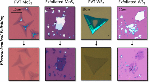
Electrochemical Polishing of Two-Dimensional Materials
ACS Nano ( IF 15.8 ) Pub Date : 2018-11-28 00:00:00 , DOI: 10.1021/acsnano.8b08216 Amritanand Sebastian 1 , Fu Zhang 2 , Akhil Dodda 1 , Dan May-Rawding 3 , He Liu 4 , Tianyi Zhang 2 , Mauricio Terrones 2, 4, 5, 6 , Saptarshi Das 1, 5
ACS Nano ( IF 15.8 ) Pub Date : 2018-11-28 00:00:00 , DOI: 10.1021/acsnano.8b08216 Amritanand Sebastian 1 , Fu Zhang 2 , Akhil Dodda 1 , Dan May-Rawding 3 , He Liu 4 , Tianyi Zhang 2 , Mauricio Terrones 2, 4, 5, 6 , Saptarshi Das 1, 5
Affiliation
|
Two-dimensional (2D) layered materials demonstrate their exquisite properties such as high temperature superconductivity, superlubricity, charge density wave, piezotronics, flextronics, straintronics, spintronics, valleytronics, and optoelectronics, mostly, at the monolayer limit. Following initial breakthroughs based on micromechanically exfoliated 2D monolayers, significant progress has been made in recent years toward the bottom-up synthesis of large-area monolayer 2D materials such as MoS2 and WS2 using physical vapor deposition and chemical vapor deposition techniques in order to facilitate their transition into commercial technologies. However, the nucleation and subsequent growth of the secondary, tertiary, and greater numbers of vertical layers poses a significant challenge not only toward the realization of uniform monolayers but also toward maintaining their consistent electronic and optoelectronic properties which change abruptly when transitioning from the monolayer to multilayer form. Chemical or physical techniques which can remove the unwanted top layers without compromising the material quality will have tremendous consequences toward the development of atomically flat, large-area, uniform monolayers of 2D materials. Here, we report a simple, elegant, and self-limiting electrochemical polishing technique that can thin down any arbitrary thickness of 2D material, irrespective of whether these are obtained using powder vapor transport or mechanical exfoliation, into their corresponding monolayer form at room temperature within a few seconds without compromising their atomistic integrity. The effectiveness of this electrochemical polishing technique is inherent to 2D transition-metal dichalcogenides owing to the stability of their basal planes, enhanced edge reactivity, and stronger than van der Waals interaction with the substrate. Our study also reveals that 2D monolayers are chemically more robust and corrosion resistant compared to their bulk counterparts in similar oxidative environments, which enables electrochemical polishing of such materials down to a monolayer.
中文翻译:

二维材料的电化学抛光
二维(2D)层状材料主要在单层极限下显示出其精美的特性,例如高温超导性,超润滑性,电荷密度波,压电,柔性电子,应变电子,自旋电子,硅谷电子和光电。在基于微机械剥离2D单层的基础上取得初步突破之后,近年来,在自底向上合成大面积单层2D材料(例如MoS 2和WS 2)方面取得了重大进展。使用物理气相沉积和化学气相沉积技术,以促进它们向商业技术的过渡。然而,第二层,第三层和大量垂直层的形核和随后的生长不仅对实现均匀的单层而且对维持其一致的电子和光电特性提出了重大挑战,当从单层过渡到单层时,电子和光电特性会突然改变。多层形式。可以去除不需要的顶层而又不影响材料质量的化学或物理技术,将对原子平面,大面积,均匀的2D材料单层膜的开发产生巨大的影响。在这里,我们报告了一种简单,优雅,以及一种自限性电化学抛光技术,该技术可以在室温下在几秒钟内将任意厚度的2D材料稀薄化,无论这些材料是使用粉末蒸汽传输还是通过机械剥落获得的,将它们制成相应的单层形式,而不会损害其原子完整性。这种电化学抛光技术的有效性是二维过渡金属二卤化物固有的,这是因为其基面的稳定性,增强的边缘反应性以及比范德华斯与基材的相互作用更强。我们的研究还表明,与类似的氧化环境中的2D单分子层相比,二维单分子层在化学上更坚固,更耐腐蚀,从而可以将此类材料电化学抛光至单分子层。
更新日期:2018-11-28
中文翻译:
二维材料的电化学抛光
二维(2D)层状材料主要在单层极限下显示出其精美的特性,例如高温超导性,超润滑性,电荷密度波,压电,柔性电子,应变电子,自旋电子,硅谷电子和光电。在基于微机械剥离2D单层的基础上取得初步突破之后,近年来,在自底向上合成大面积单层2D材料(例如MoS 2和WS 2)方面取得了重大进展。使用物理气相沉积和化学气相沉积技术,以促进它们向商业技术的过渡。然而,第二层,第三层和大量垂直层的形核和随后的生长不仅对实现均匀的单层而且对维持其一致的电子和光电特性提出了重大挑战,当从单层过渡到单层时,电子和光电特性会突然改变。多层形式。可以去除不需要的顶层而又不影响材料质量的化学或物理技术,将对原子平面,大面积,均匀的2D材料单层膜的开发产生巨大的影响。在这里,我们报告了一种简单,优雅,以及一种自限性电化学抛光技术,该技术可以在室温下在几秒钟内将任意厚度的2D材料稀薄化,无论这些材料是使用粉末蒸汽传输还是通过机械剥落获得的,将它们制成相应的单层形式,而不会损害其原子完整性。这种电化学抛光技术的有效性是二维过渡金属二卤化物固有的,这是因为其基面的稳定性,增强的边缘反应性以及比范德华斯与基材的相互作用更强。我们的研究还表明,与类似的氧化环境中的2D单分子层相比,二维单分子层在化学上更坚固,更耐腐蚀,从而可以将此类材料电化学抛光至单分子层。


 京公网安备 11010802027423号