Our official English website, www.x-mol.net, welcomes your
feedback! (Note: you will need to create a separate account there.)
Photothermally Assisted Thinning of Silicon Nitride Membranes for Ultrathin Asymmetric Nanopores
ACS Nano ( IF 15.8 ) Pub Date : 2018-11-20 00:00:00 , DOI: 10.1021/acsnano.8b06805 Hirohito Yamazaki 1 , Rui Hu 2 , Qing Zhao 2 , Meni Wanunu 1
ACS Nano ( IF 15.8 ) Pub Date : 2018-11-20 00:00:00 , DOI: 10.1021/acsnano.8b06805 Hirohito Yamazaki 1 , Rui Hu 2 , Qing Zhao 2 , Meni Wanunu 1
Affiliation
|
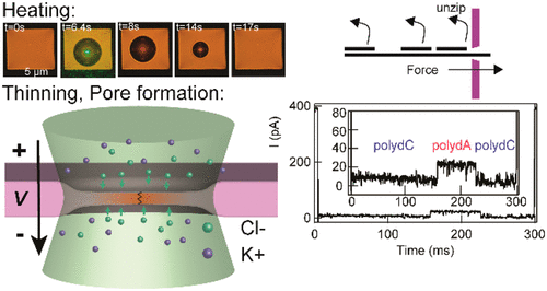
Sculpting solid-state materials at the nanoscale is an important step in the manufacturing of numerous types of sensor devices, in particular solid-state nanopore sensors. Here we present mechanistic insight into laser-induced thinning of low-stress silicon nitride (SiNx) membranes and films. In a recent study, we observed that focusing a visible wavelength laser beam on a SiNx membrane results in efficient localized heating, and we used this effect to control temperature at a solid-state nanopore sensor. A side-effect of the observed heating was that the pores expand/degrade under prolonged high-power illumination, prompting us to study the mechanism of this etching process. We find that SiNx can be etched under exposure to light of ∼107 W/cm2 average intensity, with etch rates that are influenced by the supporting electrolyte. Combining this controlled etching with dielectric breakdown, an electrokinetic process for making pores, nanopores of arbitrary dimensions as small as 1–2 nm in diameter and thickness can easily be fabricated. Evidence gathered from biomolecule-pore interactions suggests that the pore geometries obtained using this method are more funnel-like, rather than hourglass-shaped. Refined control over pore dimensions can expand the range of applications of solid-state nanopores, for example, biopolymer sequencing and detection of specific biomarkers.
中文翻译:

用于超薄不对称纳米孔的氮化硅膜的光热辅助减薄
纳米级的固态材料雕刻是制造多种类型的传感器设备(特别是固态纳米孔传感器)的重要步骤。在这里,我们介绍了对低应力氮化硅(SiN x)薄膜和薄膜进行激光诱导减薄的机械原理。在最近的一项研究中,我们观察到将可见波长的激光束聚焦在SiN x膜上会导致有效的局部加热,并且我们利用这种效应来控制固态纳米孔传感器的温度。观察到的加热的副作用是,在长时间的高功率照明下,孔会膨胀/降解,这促使我们研究这种蚀刻过程的机理。我们发现,SiN x可以在〜10 7的光下腐蚀。W / cm 2平均强度,蚀刻速率受支持电解质的影响。将这种受控刻蚀与介电击穿相结合,就可以轻松地制造出一种电动力学过程,用于制造孔径,直径和厚度小至1-2 nm的任意尺寸的纳米孔。从生物分子-孔隙相互作用中收集的证据表明,使用这种方法获得的孔的几何形状更像漏斗状,而不是沙漏状。对孔尺寸的精细控制可以扩大固态纳米孔的应用范围,例如生物聚合物测序和特定生物标记物的检测。
更新日期:2018-11-20
中文翻译:
用于超薄不对称纳米孔的氮化硅膜的光热辅助减薄
纳米级的固态材料雕刻是制造多种类型的传感器设备(特别是固态纳米孔传感器)的重要步骤。在这里,我们介绍了对低应力氮化硅(SiN x)薄膜和薄膜进行激光诱导减薄的机械原理。在最近的一项研究中,我们观察到将可见波长的激光束聚焦在SiN x膜上会导致有效的局部加热,并且我们利用这种效应来控制固态纳米孔传感器的温度。观察到的加热的副作用是,在长时间的高功率照明下,孔会膨胀/降解,这促使我们研究这种蚀刻过程的机理。我们发现,SiN x可以在〜10 7的光下腐蚀。W / cm 2平均强度,蚀刻速率受支持电解质的影响。将这种受控刻蚀与介电击穿相结合,就可以轻松地制造出一种电动力学过程,用于制造孔径,直径和厚度小至1-2 nm的任意尺寸的纳米孔。从生物分子-孔隙相互作用中收集的证据表明,使用这种方法获得的孔的几何形状更像漏斗状,而不是沙漏状。对孔尺寸的精细控制可以扩大固态纳米孔的应用范围,例如生物聚合物测序和特定生物标记物的检测。


 京公网安备 11010802027423号