Nano Energy ( IF 16.8 ) Pub Date : 2018-10-17 , DOI: 10.1016/j.nanoen.2018.10.031 Malleswararao Tangi , Jung-Wook Min , Davide Priante , Ram Chandra Subedi , Dalaver H. Anjum , Aditya Prabaswara , Nasir Alfaraj , Jian Wei Liang , Mohammad Khaled Shakfa , Tien Khee Ng , Boon S. Ooi
|
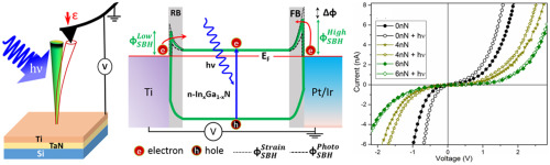
Group-III nitride nano-dimensional materials with noncentrosymmetric crystal structure offer an exciting area of piezotronics for energy conversion applications. We experimentally report the piezotronic and piezo-phototronic effects of n-InGaN nanowires (NWs) having an emission wavelength in the visible region (≈510 nm). The n-type InGaN NWs, exhibiting high structural and optical quality, were grown by plasma-assisted molecular beam epitaxy (PAMBE) on Ti/TaN/Si substrates to facilitate the direct bottom electrical contact to the NWs. Further, we use Pt/Ir conductive atomic force microscopy (c-AFM) tip as a top electrical contact to the NW. Applying compressive strain on the NWs using a c-AFM tip, the Schottky barrier height (SBH) formed at the metal-semiconductor NW interface was tuned by means of strain induced piezo-potential. Thus, we study the two-way coupling of mechanical and electrical energy results in piezotronics of n-InGaN NWs. Such measurements were further carried out under optical excitation with 405 nm laser to understand its effect on change in SBH. Thereby, we demonstrate the three-way coupling of the piezo-phototronics of n-InGaN NWs by exploiting their excellent visible optoelectronic properties. The photogenerated carriers reduce the SBH while they play a lesser role at higher tip deflection force on NWs. This revealed that at the higher strain on NW, the piezo fields screen the photoexcited carriers hence resulting in a negligible change in I-V characteristics for ≥ 6 nN tip force with and without illumination. Thus, the investigation of nanoscale piezotronic and piezo-phototronic effects of n-InGaN NWs provides an opportunity to enable piezoelectric functional devices to be used as strain-tunable, self-powered electronics and optoelectronics applications.
中文翻译:
分子束外延生长n-InGaN纳米线/ Ti中的压电和压电效应的观察
具有非中心对称晶体结构的III类氮化物纳米尺寸材料为能量转换应用提供了令人兴奋的压电技术领域。我们实验性地报告了在可见光区域(≈510nm)具有发射波长的n -InGaN纳米线(NWs)的压电和压电效应。该ñ通过等离子辅助分子束外延(PAMBE)在Ti / TaN / Si衬底上生长出具有高结构和光学质量的In型NGaN NW,以促进与NW的直接底部电接触。此外,我们使用Pt / Ir导电原子力显微镜(c-AFM)尖端作为与NW的顶部电触点。使用c-AFM尖端在NW上施加压缩应变,通过应变感应的压电势调节在金属-半导体NW界面处形成的肖特基势垒高度(SBH)。因此,我们研究了n的压电中机械能和电能的双向耦合-InGaN NW。进一步在405 nm激光的光激发下进行此类测量,以了解其对SBH变化的影响。因此,我们通过利用n -InGaN NW的出色的可见光电子特性,展示了它们的压电光电子学的三向耦合。光生载流子降低了SBH,而它们在NW上的尖端偏转力较高时起的作用较小。这表明,在NW较高的应变下,压电场屏蔽了光激发的载流子,因此在有和没有照明的情况下,对于≥6 nN的尖端力,IV特性的变化可忽略不计。因此,纳米piezotronic的调查和压电效应phototronic ñ-InGaN NW提供了将压电功能器件用作应变可调,自供电电子和光电应用的机会。


 京公网安备 11010802027423号