Our official English website, www.x-mol.net, welcomes your
feedback! (Note: you will need to create a separate account there.)
Permanent mitigation of loss in ultrathin silicon-on-insulator high-Q resonators using ultraviolet light
Optica ( IF 8.4 ) Pub Date : 2018-10-10 , DOI: 10.1364/optica.5.001271 Gioele Piccoli , Martino Bernard , Mher Ghulinyan
Optica ( IF 8.4 ) Pub Date : 2018-10-10 , DOI: 10.1364/optica.5.001271 Gioele Piccoli , Martino Bernard , Mher Ghulinyan
|
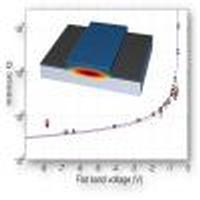
Mitigation of optical losses is of prime importance for the performance of integrated micro-photonic devices. In this paper, we demonstrate strip-loaded guiding optical components realized on a 27 nm ultra-thin silicon-on-insulator (SOI) platform. The absence of physically etched boundaries within the guiding core majorly suppresses the scattering loss, as shown by us previously for a silicon nitride () platform. Unexpectedly, the freshly fabricated Si devices showed large losses of 5.1 dB/cm originating from absorption by free carriers, accumulated under the positively charged loading layer. We show how ultraviolet (UV, 254 nm) light exposure can progressively and permanently neutralize ’s bulk charge, associated with diamagnetic defects. Consequently, the net decrease of electron concentration in the SOI layer reduces the propagation loss down to 0.9 dB/cm. Accurate cavity linewidth measurements demonstrate how the intrinsic cavity’s boosts from 70,000 up to 500,000 after UV illumination. Our results may open routes towards engineering of new functionalities in photonic devices employing UV modification of space-charge-associated local electric fields, unveil the origin of induced optical nonlinearities in micro-photonic systems, as well as envisage possible integration of these with both standard and ultra-thin SOI electronics.
中文翻译:

永久减轻超薄绝缘体上硅的高损耗
减少光损耗对于集成微光子设备的性能至关重要。在本文中,我们演示了在27 nm超薄绝缘体上硅(SOI)平台上实现的带载引导光学组件。如我们先前对氮化硅() 平台。出乎意料的是,新制作的Si器件显示出5.1 dB / cm的大损耗,这是由于自由载流子在正电荷下的吸收所导致加载层。我们展示了紫外线(UV,254 nm)曝光如何逐渐和永久中和的大电荷,与抗磁性有关 缺陷。因此,SOI层中电子浓度的净降低将传播损耗降低至0.9 dB / cm。准确的腔线宽测量表明了固有腔的紫外线照射后从70,000升至500,000。我们的结果可能为在空间电荷相关局部电场中进行UV修饰的光子器件中新功能的工程化开辟道路,揭示了感应光非线性的起源。 微光子系统,并设想将它们与标准和超薄SOI电子设备集成在一起。
更新日期:2018-10-19
中文翻译:
永久减轻超薄绝缘体上硅的高损耗
减少光损耗对于集成微光子设备的性能至关重要。在本文中,我们演示了在27 nm超薄绝缘体上硅(SOI)平台上实现的带载引导光学组件。如我们先前对氮化硅() 平台。出乎意料的是,新制作的Si器件显示出5.1 dB / cm的大损耗,这是由于自由载流子在正电荷下的吸收所导致加载层。我们展示了紫外线(UV,254 nm)曝光如何逐渐和永久中和的大电荷,与抗磁性有关 缺陷。因此,SOI层中电子浓度的净降低将传播损耗降低至0.9 dB / cm。准确的腔线宽测量表明了固有腔的紫外线照射后从70,000升至500,000。我们的结果可能为在空间电荷相关局部电场中进行UV修饰的光子器件中新功能的工程化开辟道路,揭示了感应光非线性的起源。 微光子系统,并设想将它们与标准和超薄SOI电子设备集成在一起。


 京公网安备 11010802027423号