当前位置:
X-MOL 学术
›
Chem. Mater.
›
论文详情
Our official English website, www.x-mol.net, welcomes your
feedback! (Note: you will need to create a separate account there.)
Experimental Demonstration of in Situ Stress-Driven Optical Modulations in Flexible Semiconducting Thin Films with Enhanced Photodetecting Capability
Chemistry of Materials ( IF 7.2 ) Pub Date : 2018-10-08 00:00:00 , DOI: 10.1021/acs.chemmater.8b03177 Seung Min Lee 1 , Woosun Jang 1 , Bhaskar Chandra Mohanty 2 , Jisu Yoo 3 , Jin Woo Jang 1 , Da Bin Kim 1 , Yeonjin Yi 3 , Aloysius Soon 1 , Yong Soo Cho 1
Chemistry of Materials ( IF 7.2 ) Pub Date : 2018-10-08 00:00:00 , DOI: 10.1021/acs.chemmater.8b03177 Seung Min Lee 1 , Woosun Jang 1 , Bhaskar Chandra Mohanty 2 , Jisu Yoo 3 , Jin Woo Jang 1 , Da Bin Kim 1 , Yeonjin Yi 3 , Aloysius Soon 1 , Yong Soo Cho 1
Affiliation
|
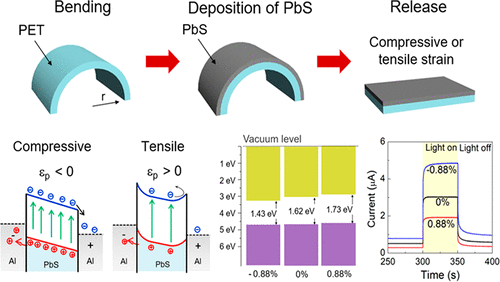
Flexible semiconducting thin films have a broad coverage of future competitive electronic and optoelectronic devices. Although the stress present in thin films has been long known to affect optical properties, the experimental verification of the optical modulations in flexible systems has not been available so far. Here, we propose an in situ deposition process of inducing intentional compressive or tensile stress in the flexible thin films, ultimately to define the actual level of optical bandgap and photosensitivity modulations using an example of narrow bandgap p-type semiconductor of PbS thin films. We experimentally and theoretically prove the stress dependency of bandgap changes from 1.43 to 1.73 eV in the strain range of −0.88 to +0.88%. A metal–semiconductor–metal device with compressive strain-induced PbS thin film exhibited a higher photoresponse compared to the unstrained ones, because of combined effects of favorable band edge positions as well as generation of a higher number of electron–hole pairs due to absorption of a wider range of photon energies owing to its lower bandgap.
中文翻译:

具有增强的光探测能力的柔性半导体薄膜中原位应力驱动光调制的实验演示
柔性半导体薄膜广泛覆盖了未来的竞争性电子和光电设备。尽管人们早就知道薄膜中存在的应力会影响光学性能,但到目前为止,尚无法对柔性系统中的光学调制进行实验验证。在此,我们提出了一种在柔性薄膜中引起有意的压缩应力或拉伸应力的原位沉积工艺,最终以PbS薄膜的窄带隙p型半导体为例,定义了光学带隙和光敏调制的实际水平。我们从实验和理论上证明了在-0.88至+ 0.88%的应变范围内,带隙的应力依赖性从1.43到1.73 eV。
更新日期:2018-10-08
中文翻译:
具有增强的光探测能力的柔性半导体薄膜中原位应力驱动光调制的实验演示
柔性半导体薄膜广泛覆盖了未来的竞争性电子和光电设备。尽管人们早就知道薄膜中存在的应力会影响光学性能,但到目前为止,尚无法对柔性系统中的光学调制进行实验验证。在此,我们提出了一种在柔性薄膜中引起有意的压缩应力或拉伸应力的原位沉积工艺,最终以PbS薄膜的窄带隙p型半导体为例,定义了光学带隙和光敏调制的实际水平。我们从实验和理论上证明了在-0.88至+ 0.88%的应变范围内,带隙的应力依赖性从1.43到1.73 eV。


 京公网安备 11010802027423号