Our official English website, www.x-mol.net, welcomes your
feedback! (Note: you will need to create a separate account there.)
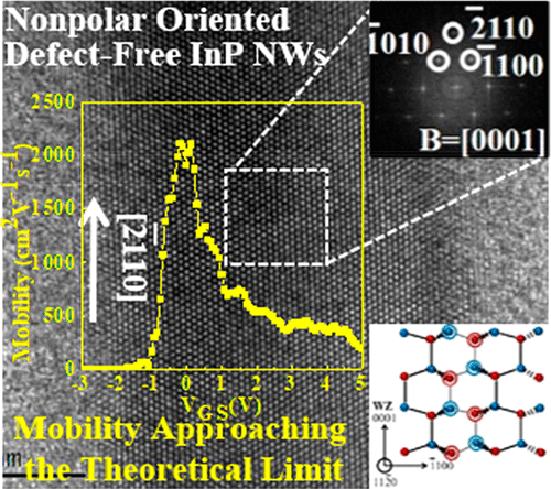
Nonpolar-Oriented Wurtzite InP Nanowires with Electron Mobility Approaching the Theoretical Limit
ACS Nano ( IF 15.8 ) Pub Date : 2018-10-04 00:00:00 , DOI: 10.1021/acsnano.8b05947 Jiamin Sun 1, 2 , Yanxue Yin 1 , Mingming Han 1 , Zai-xing Yang 1, 2 , Changyong Lan 3 , Lizhe Liu 4 , Ying Wang 5 , Ning Han 5 , Lifan Shen 3 , Xinglong Wu 4 , Johnny C. Ho 3, 6
ACS Nano ( IF 15.8 ) Pub Date : 2018-10-04 00:00:00 , DOI: 10.1021/acsnano.8b05947 Jiamin Sun 1, 2 , Yanxue Yin 1 , Mingming Han 1 , Zai-xing Yang 1, 2 , Changyong Lan 3 , Lizhe Liu 4 , Ying Wang 5 , Ning Han 5 , Lifan Shen 3 , Xinglong Wu 4 , Johnny C. Ho 3, 6
Affiliation
|
As an important semiconductor nanomaterial, InP nanowires (NWs) grown with a typical vapor–liquid–solid mechanism are still restricted from their low electron mobility for practical applications. Here, nonpolar-oriented defect-free wurtzite InP NWs with electron mobility of as high as 2000 cm2 V–1 s–1 can be successfully synthesized via Pd-catalyzed vapor–solid–solid growth. Specifically, PdIn catalyst particles are involved and found to expose their PdIn{210} planes at the InP nucleation frontier due to their minimal lattice mismatch with nonpolar InP{2̅110} and {1̅100} planes. This appropriate lattice registration would then minimize the overall free energy and enable the highly crystalline InP NW growth epitaxially along the nonpolar directions. Because of the minimized crystal defects, the record-high electron mobility of InP NWs (i.e., 2000 cm2 V–1 s–1 at an electron concentration of 1017 cm–3) results, being close to the theoretical limit of their bulk counterparts. Furthermore, once the top-gated device geometry is employed, the device subthreshold slopes can be impressively reduced down to 91 mV dec–1 at room temperature. In addition, these NWs exhibit a high photoresponsivity of 104 A W–1 with fast rise and decay times of 0.89 and 0.82 s, respectively, in photodetection. All these results evidently demonstrate the promise of nonpolar-oriented InP NWs for next-generation electronics and optoelectronics.
中文翻译:

电子迁移率接近理论极限的非极性取向纤锌矿InP纳米线
作为一种重要的半导体纳米材料,以典型的气液固机制生长的InP纳米线(NW)在实际应用中仍然受到其低电子迁移率的限制。在这里,可以通过以下方法成功合成电子迁移率高达2000 cm 2 V –1 s –1的无极性取向无缺陷纤锌矿InP NW 。钯催化的汽-固-固增长。具体地,由于PdIn催化剂颗粒与非极性InP {2̅110}和{1̅100}面的最小晶格失配,因此涉及PdIn催化剂颗粒并发现其在InP成核边界暴露其PdIn {210}面。然后,这种适当的晶格配准将使总自由能最小化,并使高度结晶的InP NW沿非极性方向外延生长。由于最小化了晶体缺陷,InP NWs的电子迁移率达到了创纪录的高水平(即,在电子浓度为10 17 cm –3的情况下为2000 cm 2 V –1 s –1)的结果,接近其同类产品的理论极限。此外,一旦采用了顶部门控的器件几何形状,在室温下,器件的亚阈值斜率就可以令人印象深刻地降低至91 mV dec –1。此外,这些NW在光电检测中表现出10 4 AW –1的高光响应性,分别具有0.89 s和0.82 s的快速上升和衰减时间。所有这些结果显然证明了面向下一代电子产品和光电产品的非极性InP NW的前景。
更新日期:2018-10-04
中文翻译:
电子迁移率接近理论极限的非极性取向纤锌矿InP纳米线
作为一种重要的半导体纳米材料,以典型的气液固机制生长的InP纳米线(NW)在实际应用中仍然受到其低电子迁移率的限制。在这里,可以通过以下方法成功合成电子迁移率高达2000 cm 2 V –1 s –1的无极性取向无缺陷纤锌矿InP NW 。钯催化的汽-固-固增长。具体地,由于PdIn催化剂颗粒与非极性InP {2̅110}和{1̅100}面的最小晶格失配,因此涉及PdIn催化剂颗粒并发现其在InP成核边界暴露其PdIn {210}面。然后,这种适当的晶格配准将使总自由能最小化,并使高度结晶的InP NW沿非极性方向外延生长。由于最小化了晶体缺陷,InP NWs的电子迁移率达到了创纪录的高水平(即,在电子浓度为10 17 cm –3的情况下为2000 cm 2 V –1 s –1)的结果,接近其同类产品的理论极限。此外,一旦采用了顶部门控的器件几何形状,在室温下,器件的亚阈值斜率就可以令人印象深刻地降低至91 mV dec –1。此外,这些NW在光电检测中表现出10 4 AW –1的高光响应性,分别具有0.89 s和0.82 s的快速上升和衰减时间。所有这些结果显然证明了面向下一代电子产品和光电产品的非极性InP NW的前景。


 京公网安备 11010802027423号