当前位置:
X-MOL 学术
›
Adv. Mater.
›
论文详情
Our official English website, www.x-mol.net, welcomes your
feedback! (Note: you will need to create a separate account there.)
Graphene/Organic Semiconductor Heterojunction Phototransistors with Broadband and Bi‐directional Photoresponse
Advanced Materials ( IF 27.4 ) Pub Date : 2018-10-01 , DOI: 10.1002/adma.201804020 Jiayue Han 1 , Jun Wang 2 , Ming Yang 1 , Xiao Kong 1 , Xiaoqing Chen 3, 4 , Zehua Huang 1 , Hui Guo 3 , Jun Gou 2 , Silu Tao 1 , Zhijun Liu 2 , Zhiming Wu 2 , Yadong Jiang 2 , Xinran Wang 4
Advanced Materials ( IF 27.4 ) Pub Date : 2018-10-01 , DOI: 10.1002/adma.201804020 Jiayue Han 1 , Jun Wang 2 , Ming Yang 1 , Xiao Kong 1 , Xiaoqing Chen 3, 4 , Zehua Huang 1 , Hui Guo 3 , Jun Gou 2 , Silu Tao 1 , Zhijun Liu 2 , Zhiming Wu 2 , Yadong Jiang 2 , Xinran Wang 4
Affiliation
|
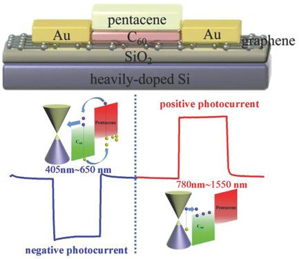
A graphene–semiconductor heterojunction is very attractive for realizing highly sensitive phototransistors due to the strong absorption of the semiconductor layer and the fast charge transport in the graphene. However, the photoresponse is usually limited to a narrow spectral range determined by the bandgap of the semiconductor. Here, an organic heterojunction (C60/pentacene) is incorporated on graphene to realize a broadband (405–1550 nm) phototransistor with a high gain of 5.2 × 10⁵ and a response time down to 275 µs. The visible and near‐infrared parts of the photoresponsivity (9127 A W−1@650 nm and 1800 A W−1@808 nm) come from the absorption of the organic layer and the graphene, respectively. For the first time, a bi‐directional (positive and negative) photoresponse is demonstrated at different wavelengths, due to the opposite charge transfer direction of the photoexcited carriers enforced by the unique band alignment. Such tunability will enable new functionalities such as large‐scale real‐time optical image and infrared focal plane array detection in the future.
中文翻译:

具有宽带和双向光响应的石墨烯/有机半导体异质结光电晶体管
石墨烯-半导体异质结由于实现了半导体层的强吸收和石墨烯中的快速电荷传输,因此对于实现高灵敏度的光电晶体管非常有吸引力。然而,光响应通常限于由半导体的带隙确定的窄光谱范围。在这里,将有机异质结(C 60 /并五苯)掺入石墨烯上,以实现宽带(405-1550 nm)光电晶体管,该晶体管具有5.2×10 5的高增益和低至275 µs的响应时间。的光响应的可见和近红外部分(9127 AW -1 @ 650nm和1800 AW -1@ 808nm)分别来自有机层和石墨烯的吸收。第一次,由于独特的能带对准,光激发载流子的电荷转移方向相反,因此在不同的波长处表现出双向(正负)光响应。这种可调性将在将来实现新功能,例如大规模实时光学图像和红外焦平面阵列检测。
更新日期:2018-10-01
中文翻译:
具有宽带和双向光响应的石墨烯/有机半导体异质结光电晶体管
石墨烯-半导体异质结由于实现了半导体层的强吸收和石墨烯中的快速电荷传输,因此对于实现高灵敏度的光电晶体管非常有吸引力。然而,光响应通常限于由半导体的带隙确定的窄光谱范围。在这里,将有机异质结(C 60 /并五苯)掺入石墨烯上,以实现宽带(405-1550 nm)光电晶体管,该晶体管具有5.2×10 5的高增益和低至275 µs的响应时间。的光响应的可见和近红外部分(9127 AW -1 @ 650nm和1800 AW -1@ 808nm)分别来自有机层和石墨烯的吸收。第一次,由于独特的能带对准,光激发载流子的电荷转移方向相反,因此在不同的波长处表现出双向(正负)光响应。这种可调性将在将来实现新功能,例如大规模实时光学图像和红外焦平面阵列检测。


 京公网安备 11010802027423号