Organic Electronics ( IF 3.2 ) Pub Date : 2018-09-26 , DOI: 10.1016/j.orgel.2018.09.041 Muhammad S. Kamaludin , Robert J. Thompson , Steve Hudziak , Oleg Mitrofanov , Neil J. Curson
|
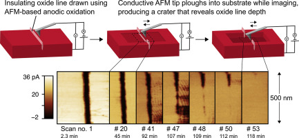
Nanopatterning electrically insulating oxide lines on organic electronic surfaces can play a role in fabricating future nanoscale devices. Here we write oxide features on rubrene single crystal surfaces by performing local anodic oxidation using the tip of an atomic force microscope. Oxide feature height increases with voltage bias and decreases with tip writing speed, and gaps as small as 22 nm at the surface between two parallel oxide lines were realised. Conductance tomography is employed in a unique way to determine the depths of oxide features, by exposing subsurface layers of the patterned material without using chemical etching while simultaneously mapping material conductance. The oxide line depth exceeds its height, with the depth-to-height ratio frequently being more than 1.6. A critical electric field of ∼3 × 10⁶ V/cm is identified, below which the oxide growth ceases, resulting in a maximum oxide vertical extent of about ∼60 nm at a voltage bias of ∼20 V.
中文翻译:
有机半导体晶体上的局部阳极氧化光刻:电导层析成像揭示的氧化物深度
在有机电子表面上对有机绝缘氧化物线进行纳米图案化可以在制造未来的纳米级器件中发挥作用。在这里,我们通过使用原子力显微镜的尖端执行局部阳极氧化,在红荧烯单晶表面上写入氧化物特征。氧化物特征高度随电压偏置而增加,并随笔尖写入速度而降低,并且在两条平行氧化物线之间的表面上实现了小至22 nm的间隙。通过在不使用化学刻蚀的情况下暴露出图案化材料的亚表面层,同时绘制材料电导,以独特的方式采用电导层析成像技术来确定氧化物特征的深度。氧化线深度超过其高度,深度高度比通常大于1.6。临界电场约为3×10 可以确定为6 V / cm,在此以下氧化物停止生长,在约20 V的电压偏置下,最大氧化物垂直延伸范围约为60 nm。


 京公网安备 11010802027423号