Our official English website, www.x-mol.net, welcomes your
feedback! (Note: you will need to create a separate account there.)
MoS2 Quantum Dot/Graphene Hybrids for Advanced Interface Engineering of a CH3NH3PbI3 Perovskite Solar Cell with an Efficiency of over 20%
ACS Nano ( IF 15.8 ) Pub Date : 2018-09-21 00:00:00 , DOI: 10.1021/acsnano.8b05514 Leyla Najafi 1 , Babak Taheri 2 , Beatriz Martín-García 1 , Sebastiano Bellani 1 , Diego Di Girolamo 2 , Antonio Agresti 2 , Reinier Oropesa-Nuñez 1, 3 , Sara Pescetelli 2 , Luigi Vesce 2 , Emanuele Calabrò 2 , Mirko Prato 4 , Antonio E. Del Rio Castillo 1 , Aldo Di Carlo 2, 5 , Francesco Bonaccorso 1, 3
ACS Nano ( IF 15.8 ) Pub Date : 2018-09-21 00:00:00 , DOI: 10.1021/acsnano.8b05514 Leyla Najafi 1 , Babak Taheri 2 , Beatriz Martín-García 1 , Sebastiano Bellani 1 , Diego Di Girolamo 2 , Antonio Agresti 2 , Reinier Oropesa-Nuñez 1, 3 , Sara Pescetelli 2 , Luigi Vesce 2 , Emanuele Calabrò 2 , Mirko Prato 4 , Antonio E. Del Rio Castillo 1 , Aldo Di Carlo 2, 5 , Francesco Bonaccorso 1, 3
Affiliation
|
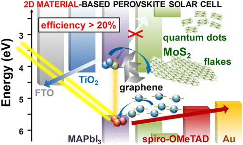
Interface engineering of organic–inorganic halide perovskite solar cells (PSCs) plays a pivotal role in achieving high power conversion efficiency (PCE). In fact, the perovskite photoactive layer needs to work synergistically with the other functional components of the cell, such as charge transporting/active buffer layers and electrodes. In this context, graphene and related two-dimensional materials (GRMs) are promising candidates to tune “on demand” the interface properties of PSCs. In this work, we fully exploit the potential of GRMs by controlling the optoelectronic properties of molybdenum disulfide (MoS2) and reduced graphene oxide (RGO) hybrids both as hole transport layer (HTL) and active buffer layer (ABL) in mesoscopic methylammonium lead iodide (CH3NH3PbI3) perovskite (MAPbI3)-based PSCs. We show that zero-dimensional MoS2 quantum dots (MoS2 QDs), derived by liquid phase exfoliated MoS2 flakes, provide both hole-extraction and electron-blocking properties. In fact, on one hand, intrinsic n-type doping-induced intraband gap states effectively extract the holes through an electron injection mechanism. On the other hand, quantum confinement effects increase the optical band gap of MoS2 (from 1.4 eV for the flakes to >3.2 eV for QDs), raising the minimum energy of its conduction band (from −4.3 eV for the flakes to −2.2 eV for QDs) above the one of the conduction band of MAPbI3 (between −3.7 and −4 eV) and hindering electron collection. The van der Waals hybridization of MoS2 QDs with functionalized reduced graphene oxide (f-RGO), obtained by chemical silanization-induced linkage between RGO and (3-mercaptopropyl)trimethoxysilane, is effective to homogenize the deposition of HTLs or ABLs onto the perovskite film, since the two-dimensional nature of RGO effectively plugs the pinholes of the MoS2 QD films. Our “graphene interface engineering” (GIE) strategy based on van der Waals MoS2 QD/graphene hybrids enables MAPbI3-based PSCs to achieve a PCE up to 20.12% (average PCE of 18.8%). The possibility to combine quantum and chemical effects into GIE, coupled with the recent success of graphene and GRMs as interfacial layer, represents a promising approach for the development of next-generation PSCs.
中文翻译:

MoS 2量子点/石墨烯杂化物,用于CH 3 NH 3 PbI 3钙钛矿太阳能电池的高级接口工程,效率超过20%
有机-无机卤化物钙钛矿太阳能电池(PSC)的界面工程在实现高功率转换效率(PCE)中起着关键作用。实际上,钙钛矿光敏层需要与电池的其他功能组件(例如电荷传输/活性缓冲层和电极)协同工作。在这种情况下,石墨烯和相关的二维材料(GRM)是有望“按需”调整PSC界面特性的候选材料。在这项工作中,我们通过控制二硫化钼(MoS 2)和还原性氧化石墨烯(RGO)杂化物的光电性能,充分利用了GRM的潜力,这些杂物既用作介电层甲基铵铅中的空穴传输层(HTL),又用作有源缓冲层(ABL)。碘化物(CH 3 NH 3碘化铅3)钙钛矿(MAPbI 3)为基础的产品分成合同。我们表明,由液相剥落的MoS 2薄片衍生的零维MoS 2量子点(MoS 2 QDs)提供了空穴提取和电子阻挡特性。实际上,一方面,固有的n型掺杂引起的带内能隙状态通过电子注入机制有效地提取了空穴。另一方面,量子约束效应增加了MoS 2的光学带隙(从薄片的1.4 eV到QD的> 3.2 eV),从而提高了其导带的最小能量(从薄片的-4.3 eV到-2.2 QDs的eV)高于MAPbI 3的导带之一(在-3.7和-4 eV之间)并阻碍电子收集。通过化学硅烷化诱导RGO和(3-巯基丙基)三甲氧基硅烷之间的键合获得的MoS 2 QD与功能化还原氧化石墨烯(f-RGO)的范德华杂交,可以有效地使HTL或ABL沉积在钙钛矿上由于RGO的二维性质有效地堵塞了MoS 2 QD膜的针孔。我们基于van der Waals MoS 2 QD /石墨烯混合物的“石墨烯界面工程”(GIE)策略可实现MAPbI 3的PSC,以实现高达20.12%的PCE(平均PCE为18.8%)。将量子和化学效应结合到GIE中的可能性,以及石墨烯和GRM作为界面层的最新成功,代表了开发下一代PSC的有前途的方法。
更新日期:2018-09-21
中文翻译:
MoS 2量子点/石墨烯杂化物,用于CH 3 NH 3 PbI 3钙钛矿太阳能电池的高级接口工程,效率超过20%
有机-无机卤化物钙钛矿太阳能电池(PSC)的界面工程在实现高功率转换效率(PCE)中起着关键作用。实际上,钙钛矿光敏层需要与电池的其他功能组件(例如电荷传输/活性缓冲层和电极)协同工作。在这种情况下,石墨烯和相关的二维材料(GRM)是有望“按需”调整PSC界面特性的候选材料。在这项工作中,我们通过控制二硫化钼(MoS 2)和还原性氧化石墨烯(RGO)杂化物的光电性能,充分利用了GRM的潜力,这些杂物既用作介电层甲基铵铅中的空穴传输层(HTL),又用作有源缓冲层(ABL)。碘化物(CH 3 NH 3碘化铅3)钙钛矿(MAPbI 3)为基础的产品分成合同。我们表明,由液相剥落的MoS 2薄片衍生的零维MoS 2量子点(MoS 2 QDs)提供了空穴提取和电子阻挡特性。实际上,一方面,固有的n型掺杂引起的带内能隙状态通过电子注入机制有效地提取了空穴。另一方面,量子约束效应增加了MoS 2的光学带隙(从薄片的1.4 eV到QD的> 3.2 eV),从而提高了其导带的最小能量(从薄片的-4.3 eV到-2.2 QDs的eV)高于MAPbI 3的导带之一(在-3.7和-4 eV之间)并阻碍电子收集。通过化学硅烷化诱导RGO和(3-巯基丙基)三甲氧基硅烷之间的键合获得的MoS 2 QD与功能化还原氧化石墨烯(f-RGO)的范德华杂交,可以有效地使HTL或ABL沉积在钙钛矿上由于RGO的二维性质有效地堵塞了MoS 2 QD膜的针孔。我们基于van der Waals MoS 2 QD /石墨烯混合物的“石墨烯界面工程”(GIE)策略可实现MAPbI 3的PSC,以实现高达20.12%的PCE(平均PCE为18.8%)。将量子和化学效应结合到GIE中的可能性,以及石墨烯和GRM作为界面层的最新成功,代表了开发下一代PSC的有前途的方法。


 京公网安备 11010802027423号