当前位置:
X-MOL 学术
›
Small Methods
›
论文详情
Our official English website, www.x-mol.net, welcomes your
feedback! (Note: you will need to create a separate account there.)
Direct Visualization of Grain Boundaries in 2D Monolayer WS2 via Induced Growth of CdS Nanoparticle Chains
Small Methods ( IF 10.7 ) Pub Date : 2018-09-14 , DOI: 10.1002/smtd.201800245 Changyong Lan 1, 2 , Dapan Li 1, 3 , Ziyao Zhou 1, 3 , SenPo Yip 1, 3, 4 , Heng Zhang 1, 3 , Lei Shu 1, 3, 4 , Renjie Wei 1, 3 , Ruoting Dong 1 , Johnny C. Ho 1, 3, 4, 5
Small Methods ( IF 10.7 ) Pub Date : 2018-09-14 , DOI: 10.1002/smtd.201800245 Changyong Lan 1, 2 , Dapan Li 1, 3 , Ziyao Zhou 1, 3 , SenPo Yip 1, 3, 4 , Heng Zhang 1, 3 , Lei Shu 1, 3, 4 , Renjie Wei 1, 3 , Ruoting Dong 1 , Johnny C. Ho 1, 3, 4, 5
Affiliation
|
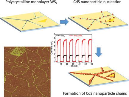
To date, wafer‐scale synthesis of two‐dimensional (2D) materials are well achieved by chemical vapor deposition, but the obtained monolayers typically have multidomains with electrical and optoelectronic properties affected by grain boundaries and domain sizes. When these 2D materials are used as the growth templates, these boundaries would also provide unknown influences to the successive heterostructure formation for extended applications. Here, for the first time, direct visualization of grain boundaries in monolayer WS2 film can be realized by the growth of CdS nanoparticles. Specifically, CdS is found to first preferentially nucleate and form as nanoparticle chains along WS2 grain boundaries in a random manner, independent of the grain boundary characteristics. Due to electron scattering and type II band alignment at the WS2–CdS heterojunction, WS2 reduces in its mobility while becoming enhanced in its electron concentration. Notably, the WS2–CdS heterostructure also yields improved carrier separation and collection for the photodetection performance enhancement. All these results can facilitate the detailed evaluation of crystalline grains‐related information of 2D materials and provide thorough understanding on the effect of these overgrown CdS on underlying WS2 monolayers, being extremely important to further optimize and enable their functionalities for advanced device applications.
中文翻译:

通过诱导CdS纳米粒子链的生长直接可视化二维单层WS2中的晶界
迄今为止,通过化学气相沉积已很好地实现了二维(2D)材料的晶圆级合成,但是获得的单层通常具有多畴,该多畴的电和光电子特性受晶界和畴尺寸的影响。当将这些2D材料用作生长模板时,这些边界还将对扩展应用中的后续异质结构形成提供未知的影响。在这里,第一次,通过CdS纳米粒子的生长可以实现单层WS 2膜中晶界的直接可视化。具体而言,发现CdS首先优先成核并沿着WS 2形成纳米颗粒链晶界以随机方式存在,与晶界特征无关。由于WS 2 -CdS异质结处的电子散射和II型能带对准,WS 2的迁移率降低,同时电子浓度增强。值得注意的是,WS 2 –CdS异质结构还改善了载流子的分离和收集,从而增强了光检测性能。所有这些结果可以促进对2D材料的晶粒相关信息的详细评估,并提供对这些过度生长的CdS对基础WS 2单层的影响的透彻了解,对于进一步优化和启用其功能以用于高级设备应用极为重要。
更新日期:2018-09-14
中文翻译:
通过诱导CdS纳米粒子链的生长直接可视化二维单层WS2中的晶界
迄今为止,通过化学气相沉积已很好地实现了二维(2D)材料的晶圆级合成,但是获得的单层通常具有多畴,该多畴的电和光电子特性受晶界和畴尺寸的影响。当将这些2D材料用作生长模板时,这些边界还将对扩展应用中的后续异质结构形成提供未知的影响。在这里,第一次,通过CdS纳米粒子的生长可以实现单层WS 2膜中晶界的直接可视化。具体而言,发现CdS首先优先成核并沿着WS 2形成纳米颗粒链晶界以随机方式存在,与晶界特征无关。由于WS 2 -CdS异质结处的电子散射和II型能带对准,WS 2的迁移率降低,同时电子浓度增强。值得注意的是,WS 2 –CdS异质结构还改善了载流子的分离和收集,从而增强了光检测性能。所有这些结果可以促进对2D材料的晶粒相关信息的详细评估,并提供对这些过度生长的CdS对基础WS 2单层的影响的透彻了解,对于进一步优化和启用其功能以用于高级设备应用极为重要。


 京公网安备 11010802027423号