当前位置:
X-MOL 学术
›
Adv. Mater.
›
论文详情
Our official English website, www.x-mol.net, welcomes your
feedback! (Note: you will need to create a separate account there.)
Large‐Area Synthesis of Layered HfS2(1−x)Se2x Alloys with Fully Tunable Chemical Compositions and Bandgaps
Advanced Materials ( IF 27.4 ) Pub Date : 2018-09-14 , DOI: 10.1002/adma.201803285 Denggui Wang 1, 2 , Xingwang Zhang 1, 2 , Gencai Guo 3 , Shihan Gao 1, 2 , Xingxing Li 1, 2 , Junhua Meng 1, 2 , Zhigang Yin 1, 2 , Heng Liu 1, 2 , Menglei Gao 1, 2 , Likun Cheng 1, 2 , Jingbi You 1, 2 , Ruzhi Wang 3
Advanced Materials ( IF 27.4 ) Pub Date : 2018-09-14 , DOI: 10.1002/adma.201803285 Denggui Wang 1, 2 , Xingwang Zhang 1, 2 , Gencai Guo 3 , Shihan Gao 1, 2 , Xingxing Li 1, 2 , Junhua Meng 1, 2 , Zhigang Yin 1, 2 , Heng Liu 1, 2 , Menglei Gao 1, 2 , Likun Cheng 1, 2 , Jingbi You 1, 2 , Ruzhi Wang 3
Affiliation
|
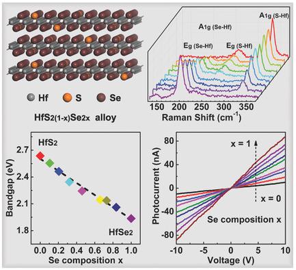
Alloying transition metal dichalcogenides (TMDs) with different compositions is demonstrated as an effective way to acquire 2D semiconductors with widely tunable bandgaps. Herein, for the first time, the large‐area synthesis of layered HfS2(1−x)Se2x alloys with fully tunable chemical compositions on sapphire by chemical vapor deposition is reported, greatly expanding and enriching the family of 2D TMDs semiconductors. The configuration and high quality of their crystal structure are confirmed by various characterization techniques, and the bandgap of these alloys can be continually modulated from 2.64 to 1.94 eV with composition variations. Furthermore, prototype HfS2(1−x)Se2x photodetectors with different Se compositions are fabricated, and the HfSe2 photodetector manifests the best performance among all the tested HfS2(1−x)Se2x devices. Remarkably, by introducing a hexagonal boron nitride layer, the performance of the HfSe2 photodetector is greatly improved, exhibiting a high on/off ratio exceeding 105, an ultrafast response time of about 190 µs, and a high detectivity of 1012 Jones. This simple and controllable approach opens up a new way to produce high‐quality 2D HfS2(1−x)Se2x layers, which are highly qualified candidates for the next‐generation application in high‐performance optoelectronics.
中文翻译:

具有完全可调的化学成分和带隙的层状HfS2(1-x)Se2x合金的大面积合成
合金化具有不同组成的过渡金属二硫化碳(TMD)被证明是获得带宽可调带隙的2D半导体的有效方法。本文首次报道了通过化学气相沉积在蓝宝石上通过化学气相沉积法对具有完全可调的化学成分的层状HfS 2(1- x) Se 2 x合金进行大面积合成的方法,极大地扩展和丰富了2D TMDs半导体家族。各种表征技术证实了它们的晶体结构和高质量的晶体结构,并且这些合金的带隙可以在2.64至1.94 eV的范围内连续变化,且成分也有所变化。此外,原型HfS 2(1- x) Se 2制作了x个具有不同Se组成的光电探测器,HfSe 2光电探测器在所有测试的HfS 2(1- x) Se 2 x器件中表现出最好的性能。显着地,通过引入六方氮化硼层,HfSe 2光电探测器的性能得到了极大的改善,表现出超过10 5的高开/关比,约190 µs的超快响应时间,以及10 12 Jones的高检测率。这种简单且可控的方法为生产高质量2D HfS 2(1- x) Se 2 x开辟了一条新途径。 层,是高性能光电电子的下一代应用的高度合格的候选人。
更新日期:2018-09-14
中文翻译:
具有完全可调的化学成分和带隙的层状HfS2(1-x)Se2x合金的大面积合成
合金化具有不同组成的过渡金属二硫化碳(TMD)被证明是获得带宽可调带隙的2D半导体的有效方法。本文首次报道了通过化学气相沉积在蓝宝石上通过化学气相沉积法对具有完全可调的化学成分的层状HfS 2(1- x) Se 2 x合金进行大面积合成的方法,极大地扩展和丰富了2D TMDs半导体家族。各种表征技术证实了它们的晶体结构和高质量的晶体结构,并且这些合金的带隙可以在2.64至1.94 eV的范围内连续变化,且成分也有所变化。此外,原型HfS 2(1- x) Se 2制作了x个具有不同Se组成的光电探测器,HfSe 2光电探测器在所有测试的HfS 2(1- x) Se 2 x器件中表现出最好的性能。显着地,通过引入六方氮化硼层,HfSe 2光电探测器的性能得到了极大的改善,表现出超过10 5的高开/关比,约190 µs的超快响应时间,以及10 12 Jones的高检测率。这种简单且可控的方法为生产高质量2D HfS 2(1- x) Se 2 x开辟了一条新途径。 层,是高性能光电电子的下一代应用的高度合格的候选人。


 京公网安备 11010802027423号