当前位置:
X-MOL 学术
›
Adv. Mater.
›
论文详情
Our official English website, www.x-mol.net, welcomes your
feedback! (Note: you will need to create a separate account there.)
High Mobilities in Layered InSe Transistors with Indium‐Encapsulation‐Induced Surface Charge Doping
Advanced Materials ( IF 27.4 ) Pub Date : 2018-09-14 , DOI: 10.1002/adma.201803690 Mengjiao Li,Che-Yi Lin,Shih-Hsien Yang,Yuan-Ming Chang,Jen-Kuei Chang,Feng-Shou Yang,Chaorong Zhong,Wen-Bin Jian,Chen-Hsin Lien,Ching-Hwa Ho,Heng-Jui Liu,Rong Huang,Wenwu Li,Yen-Fu Lin,Junhao Chu
Advanced Materials ( IF 27.4 ) Pub Date : 2018-09-14 , DOI: 10.1002/adma.201803690 Mengjiao Li,Che-Yi Lin,Shih-Hsien Yang,Yuan-Ming Chang,Jen-Kuei Chang,Feng-Shou Yang,Chaorong Zhong,Wen-Bin Jian,Chen-Hsin Lien,Ching-Hwa Ho,Heng-Jui Liu,Rong Huang,Wenwu Li,Yen-Fu Lin,Junhao Chu
|
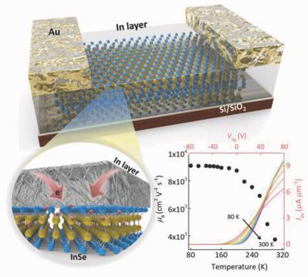
Tunability and stability in the electrical properties of 2D semiconductors pave the way for their practical applications in logic devices. A robust layered indium selenide (InSe) field‐effect transistor (FET) with superior controlled stability is demonstrated by depositing an indium (In) doping layer. The optimized InSe FETs deliver an unprecedented high electron mobility up to 3700 cm2 V−1 s−1 at room temperature, which can be retained with 60% after 1 month. Further insight into the evolution of the position of the Fermi level and the microscopic device structure with different In thicknesses demonstrates an enhanced electron‐doping behavior at the In/InSe interface. Furthermore, the contact resistance is also improved through the In insertion between InSe and Au electrodes, which coincides with the analysis of the low‐frequency noise. The carrier fluctuation is attributed to the dominance of the phonon scattering events, which agrees with the observation of the temperature‐dependent mobility. Finally, the flexible functionalities of the logic‐circuit applications, for instance, inverter and not‐and (NAND)/not‐or (NOR) gates, are determined with these surface‐doping InSe FETs, which establish a paradigm for 2D‐based materials to overcome the bottleneck in the development of electronic devices.
中文翻译:

铟封装诱导表面电荷掺杂的层状InSe晶体管的高迁移率
2D半导体的电特性的可调性和稳定性为其在逻辑设备中的实际应用铺平了道路。通过沉积铟(In)掺杂层,可以证明具有鲁棒性的层状硒化铟(InSe)场效应晶体管(FET)的稳定性。经过优化的InSe FET可提供高达3700 cm 2 V -1 s -1的前所未有的高电子迁移率在室温下,可在1个月后保留60%。进一步了解费米能级位置的变化以及具有不同In厚度的微观器件结构,证明了In / InSe界面处电子掺杂行为的增强。此外,通过InSe和Au电极之间的In插入,还提高了接触电阻,这与分析低频噪声相吻合。载流子的波动归因于声子散射事件的优势,这与对温度依赖性迁移率的观察一致。最后,这些表面掺杂InSe FET决定了逻辑电路应用的灵活功能,例如反相器和非与(NAND)/非或(NOR)门,
更新日期:2018-09-14
中文翻译:
铟封装诱导表面电荷掺杂的层状InSe晶体管的高迁移率
2D半导体的电特性的可调性和稳定性为其在逻辑设备中的实际应用铺平了道路。通过沉积铟(In)掺杂层,可以证明具有鲁棒性的层状硒化铟(InSe)场效应晶体管(FET)的稳定性。经过优化的InSe FET可提供高达3700 cm 2 V -1 s -1的前所未有的高电子迁移率在室温下,可在1个月后保留60%。进一步了解费米能级位置的变化以及具有不同In厚度的微观器件结构,证明了In / InSe界面处电子掺杂行为的增强。此外,通过InSe和Au电极之间的In插入,还提高了接触电阻,这与分析低频噪声相吻合。载流子的波动归因于声子散射事件的优势,这与对温度依赖性迁移率的观察一致。最后,这些表面掺杂InSe FET决定了逻辑电路应用的灵活功能,例如反相器和非与(NAND)/非或(NOR)门,


 京公网安备 11010802027423号