Our official English website, www.x-mol.net, welcomes your
feedback! (Note: you will need to create a separate account there.)
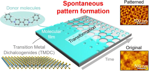
Tuning Transition-Metal Dichalcogenide Field-Effect Transistors by Spontaneous Pattern Formation of an Ultrathin Molecular Dopant Film
ACS Nano ( IF 15.8 ) Pub Date : 2018-09-14 00:00:00 , DOI: 10.1021/acsnano.8b04914 Hisashi Ichimiya 1 , Masahiro Takinoue 2 , Akito Fukui 1 , Kohei Miura 1 , Takeshi Yoshimura 1 , Atsushi Ashida 1 , Norifumi Fujimura 1 , Daisuke Kiriya 1, 3
ACS Nano ( IF 15.8 ) Pub Date : 2018-09-14 00:00:00 , DOI: 10.1021/acsnano.8b04914 Hisashi Ichimiya 1 , Masahiro Takinoue 2 , Akito Fukui 1 , Kohei Miura 1 , Takeshi Yoshimura 1 , Atsushi Ashida 1 , Norifumi Fujimura 1 , Daisuke Kiriya 1, 3
Affiliation
|
Spontaneous pattern formation is an energetically favorable process and is shown in nature in molecular-scale assembly, biological association, and soft material organizations. The opposite regime, the artificial process, which is widely applied to the fabrication of semiconducting devices, such as lithographic techniques, requires enormous amounts of energy. Here, we propose a concept of tuning the properties of semiconducting MoS2 and WSe2 devices using the spontaneous pattern formation of adjacent molecular films. The film used was a 10 nm thick ultrathin film of a molecular electron dopant, which exhibited spontaneous pattern formation and dynamically transformed the morphology of tiny holes, a network, a maze, and dots on substrates, including SiO2, MoS2, and WSe2. These patterns were exhibited only when the film came in contact with water and was tuned with temperature and time. The specific lengths of the patterns were less than 200 nm, which is sufficiently smaller than the exfoliated ∼10 μm semiconducting MoS2 and WSe2 flakes. The properties of the field-effect devices of MoS2 and WSe2 were found to be modified according to the pattern formation process of the ultrathin molecular film on the device. This concept applies the spontaneous patterning phenomena shown in nature to the fabrication and optimization of electronic devices by using molecular films and their responses to the external environment.
中文翻译:

通过超薄分子掺杂剂薄膜的自发形成来调谐过渡金属双硫族化物场效应晶体管
自发形成图案是在能量上有利的过程,并且在分子规模的组装,生物缔合和柔软的材料组织中被自然显示。相反的方法是人工过程,它广泛应用于半导体器件的制造,例如光刻技术,它需要大量的能量。在这里,我们提出了一种利用相邻分子膜的自发图案形成来调节半导体MoS 2和WSe 2器件性能的概念。使用的膜是分子电子掺杂剂的10 nm厚的超薄膜,该膜表现出自发的图案形成,并动态改变了包括SiO 2,MoS在内的基板上的小孔,网络,迷宫和点的形态2和WSe 2。这些图案仅在薄膜与水接触并随温度和时间调整后才显示出来。图案的特定长度小于200nm,其充分小于剥落的〜10μm的半导体MoS 2和WSe 2薄片。发现MoS 2和WSe 2的场效应器件的性能根据器件上超薄分子膜的图案形成过程进行了修改。该概念通过使用分子膜及其对外部环境的响应,将自然界中显示的自然图案现象应用于电子设备的制造和优化。
更新日期:2018-09-14
中文翻译:
通过超薄分子掺杂剂薄膜的自发形成来调谐过渡金属双硫族化物场效应晶体管
自发形成图案是在能量上有利的过程,并且在分子规模的组装,生物缔合和柔软的材料组织中被自然显示。相反的方法是人工过程,它广泛应用于半导体器件的制造,例如光刻技术,它需要大量的能量。在这里,我们提出了一种利用相邻分子膜的自发图案形成来调节半导体MoS 2和WSe 2器件性能的概念。使用的膜是分子电子掺杂剂的10 nm厚的超薄膜,该膜表现出自发的图案形成,并动态改变了包括SiO 2,MoS在内的基板上的小孔,网络,迷宫和点的形态2和WSe 2。这些图案仅在薄膜与水接触并随温度和时间调整后才显示出来。图案的特定长度小于200nm,其充分小于剥落的〜10μm的半导体MoS 2和WSe 2薄片。发现MoS 2和WSe 2的场效应器件的性能根据器件上超薄分子膜的图案形成过程进行了修改。该概念通过使用分子膜及其对外部环境的响应,将自然界中显示的自然图案现象应用于电子设备的制造和优化。


 京公网安备 11010802027423号