Journal of Colloid and Interface Science ( IF 9.4 ) Pub Date : 2018-09-13 , DOI: 10.1016/j.jcis.2018.09.040 Sozaraj Rasappa , Hanna Hulkkonen , Lars Schulte , Sokol Ndoni , Jarno Reuna , Turkka Salminen , Tapio Niemi
|
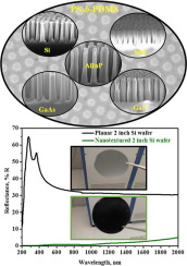
An unusual dot pattern was realized via self-assembly of high molecular weight polystyrene-block-polydimethylsiloxane (PS-b-PDMS) copolymer by a simple one-step solvent annealing process, optimized based on Hansen solubility parameters. Annealing PS-b-PDMS under neutral solvent vapors at room temperature produces an ordered arrangement of dots with ∼112 nm spacing and ∼54 nm diameter. The template is highly resistant to dry etching with chlorine-based plasma, enabling its utilization on a variety of hard masks and substrates. The self-assembled PDMS dots were further exploited as a template for direct patterning of silicon, metal, and dielectric materials. This nanopatterning methodology circumvents expensive and time-consuming atomic layer deposition, wet processes, and sequential infiltration techniques. Application-wise, we show a process to fabricate nanostructured antireflection surfaces (nanocones) on a 2 in. silicon wafer, reducing the reflectance of planar silicon from 35% to below 0.5% over a broad wavelength range. Alternatively, nanocones made of TiO2 on silicon exhibit low reflectance (<3%) and improved transmittance into the substrate at the visible wavelength range. The measured optical properties concur with the simulation results. The versatility of the PS-b-PDMS templates was further utilized for nanopatterning materials such as silicon-on-insulator substrates, gallium arsenide, aluminum indium phosphide, and gallium nitride, which are important in electronics and photonics.
中文翻译:
用于硬掩模和光子纳米结构纳米加工的高分子量嵌段共聚物光刻
通过基于Hansen溶解度参数优化的简单的一步溶剂退火工艺,通过高分子量聚苯乙烯-嵌段-聚二甲基硅氧烷(PS- b -PDMS)共聚物的自组装,实现了不寻常的点图案。退火PS- b-PDMS在室温下在中性溶剂蒸汽下产生的点的排列有序,间距为〜112 nm,直径为〜54 nm。该模板具有很高的耐氯基等离子体干法蚀刻性能,可在各种硬掩模和基板上使用。自组装的PDMS点被进一步用作直接图案化硅,金属和介电材料的模板。这种纳米图案化方法规避了昂贵且费时的原子层沉积,湿法工艺和顺序渗透技术。在应用方面,我们展示了一种在2英寸硅晶片上制造纳米结构抗反射表面(纳米酮)的工艺,可将平面硅的反射率在较宽的波长范围内从35%降低至0.5%以下。或者,由TiO 2制成的纳米锥在可见光波长范围内,硅上的硅片显示出低反射率(<3%)并提高了对基板的透射率。测得的光学性质与仿真结果一致。PS- b -PDMS模板的多功能性进一步用于纳米图案化材料,例如绝缘体上硅衬底,砷化镓,磷化铝铟和氮化镓,它们在电子和光子学中很重要。


 京公网安备 11010802027423号