Our official English website, www.x-mol.net, welcomes your
feedback! (Note: you will need to create a separate account there.)
Field-Effect Device Using Quasi-Two-Dimensional Electron Gas in Mass-Producible Atomic-Layer-Deposited Al2O3/TiO2 Ultrathin (<10 nm) Film Heterostructures
ACS Nano ( IF 15.8 ) Pub Date : 2018-09-11 00:00:00 , DOI: 10.1021/acsnano.8b05891 Tae Jun Seok , Yuhang Liu , Hae Jun Jung 1 , Soo Bin Kim 1 , Dae Hyun Kim , Sung Min Kim 1 , Jae Hyuck Jang 2 , Deok-Yong Cho 3 , Sang Woon Lee 1 , Tae Joo Park
ACS Nano ( IF 15.8 ) Pub Date : 2018-09-11 00:00:00 , DOI: 10.1021/acsnano.8b05891 Tae Jun Seok , Yuhang Liu , Hae Jun Jung 1 , Soo Bin Kim 1 , Dae Hyun Kim , Sung Min Kim 1 , Jae Hyuck Jang 2 , Deok-Yong Cho 3 , Sang Woon Lee 1 , Tae Joo Park
Affiliation
|
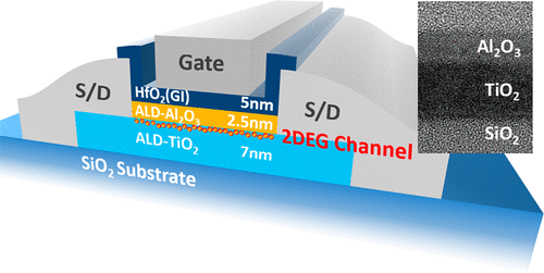
We report the field-effect transistors using quasi-two-dimensional electron gas generated at an ultrathin (∼10 nm) Al2O3/TiO2 heterostructure interface grown via atomic layer deposition (ALD) on a SiO2/Si substrate without using a single crystal substrate. The 2DEG at the Al2O3/TiO2 interface originates from oxygen vacancies generated at the surface of the TiO2 bottom layer during ALD of the Al2O3 overlayer. High-density electrons (∼1014 cm–2) are confined within a ∼2.2 nm distance from the Al2O3/TiO2 interface, resulting in a high on-current of ∼12 μA/μm. The ultrathin TiO2 bottom layer is easy to fully deplete, allowing an extremely low off-current, a high on/off current ratio over 108, and a low subthreshold swing of ∼100 mV/decade. Via the implementation of ALD, a mature thin-film process can facilitate mass production as well as three-dimensional integration of the devices.
中文翻译:

在可大量生产的原子层沉积Al 2 O 3 / TiO 2超薄(<10 nm)薄膜异质结构中使用准二维电子气的场效应器件
我们报告了使用通过在SiO 2 / Si基板上通过原子层沉积(ALD)生长的超薄(〜10 nm)Al 2 O 3 / TiO 2异质结构界面生成的准二维电子气产生的场效应晶体管,而无需使用单晶衬底。Al 2 O 3 / TiO 2界面处的2DEG源于Al 2 O 3覆盖层的ALD过程中在TiO 2底层表面产生的氧空位。高密度电子(〜10 14 cm –2)被限制在距离Al约2.2 nm的范围内2 O 3 / TiO 2界面,导致约12μA/μm的高导通电流。极薄的TiO 2底层很容易完全耗尽,允许极低的截止电流,超过10 8的高导通/截止电流比以及低至约100 mV /十倍的亚阈值摆幅。通过ALD的实施,成熟的薄膜工艺可以促进批量生产以及器件的三维集成。
更新日期:2018-09-11
中文翻译:
在可大量生产的原子层沉积Al 2 O 3 / TiO 2超薄(<10 nm)薄膜异质结构中使用准二维电子气的场效应器件
我们报告了使用通过在SiO 2 / Si基板上通过原子层沉积(ALD)生长的超薄(〜10 nm)Al 2 O 3 / TiO 2异质结构界面生成的准二维电子气产生的场效应晶体管,而无需使用单晶衬底。Al 2 O 3 / TiO 2界面处的2DEG源于Al 2 O 3覆盖层的ALD过程中在TiO 2底层表面产生的氧空位。高密度电子(〜10 14 cm –2)被限制在距离Al约2.2 nm的范围内2 O 3 / TiO 2界面,导致约12μA/μm的高导通电流。极薄的TiO 2底层很容易完全耗尽,允许极低的截止电流,超过10 8的高导通/截止电流比以及低至约100 mV /十倍的亚阈值摆幅。通过ALD的实施,成熟的薄膜工艺可以促进批量生产以及器件的三维集成。


 京公网安备 11010802027423号