当前位置:
X-MOL 学术
›
Adv. Funct. Mater.
›
论文详情
Our official English website, www.x-mol.net, welcomes your
feedback! (Note: you will need to create a separate account there.)
All‐Solid‐State Synaptic Transistor with Ultralow Conductance for Neuromorphic Computing
Advanced Functional Materials ( IF 18.5 ) Pub Date : 2018-09-05 , DOI: 10.1002/adfm.201804170 Chuan-Sen Yang 1 , Da-Shan Shang 1 , Nan Liu 1 , Elliot J. Fuller 2 , Sapan Agrawal 2 , A. Alec Talin 2 , Yong-Qing Li 1 , Bao-Gen Shen 1 , Young Sun 1
Advanced Functional Materials ( IF 18.5 ) Pub Date : 2018-09-05 , DOI: 10.1002/adfm.201804170 Chuan-Sen Yang 1 , Da-Shan Shang 1 , Nan Liu 1 , Elliot J. Fuller 2 , Sapan Agrawal 2 , A. Alec Talin 2 , Yong-Qing Li 1 , Bao-Gen Shen 1 , Young Sun 1
Affiliation
|
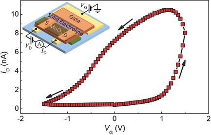
Electronic synaptic devices are important building blocks for neuromorphic computational systems that can go beyond the constraints of von Neumann architecture. Although two‐terminal memristive devices are demonstrated to be possible candidates, they suffer from several shortcomings related to the filament formation mechanism including nonlinear switching, write noise, and high device conductance, all of which limit the accuracy and energy efficiency. Electrochemical three‐terminal transistors, in which the channel conductance can be tuned without filament formation provide an alternative platform for synaptic electronics. Here, an all‐solid‐state electrochemical transistor made with Li ion–based solid dielectric and 2D α‐phase molybdenum oxide (α‐MoO3) nanosheets as the channel is demonstrated. These devices achieve nonvolatile conductance modulation in an ultralow conductance regime (<75 nS) by reversible intercalation of Li ions into the α‐MoO3 lattice. Based on this operating mechanism, the essential functionalities of synapses, such as short‐ and long‐term synaptic plasticity and bidirectional near‐linear analog weight update are demonstrated. Simulations using the handwritten digit data sets demonstrate high recognition accuracy (94.1%) of the synaptic transistor arrays. These results provide an insight into the application of 2D oxides for large‐scale, energy‐efficient neuromorphic computing networks.
中文翻译:

具有超低电导的全固态突触晶体管,用于神经形态计算
电子突触设备是神经形态计算系统的重要构建模块,可以超越冯·诺依曼体系结构的限制。尽管已证明两端忆阻器件是可能的候选器件,但它们具有与灯丝形成机制相关的若干缺点,包括非线性切换,写入噪声和高器件电导率,所有这些均限制了精度和能效。电化学三端晶体管,其中的通道电导可以在不形成灯丝的情况下进行调节,为突触电子学提供了另一种平台。在这里,是一种全固态电化学晶体管,它由基于锂离子的固体电介质和二维α相氧化钼(α‐MoO 3)展示了纳米片作为通道。这些装置实现由Li离子的可逆性嵌入到α-的MoO在超低电导体制(<75个NS)非易失性电导调制3晶格。基于这种操作机制,证明了突触的基本功能,例如短期和长期突触可塑性和双向近线性模拟权重更新。使用手写数字数据集进行的仿真表明,突触晶体管阵列的识别率很高(94.1%)。这些结果为二维氧化物在大规模,节能高效的神经形态计算网络中的应用提供了见识。
更新日期:2018-09-05
中文翻译:
具有超低电导的全固态突触晶体管,用于神经形态计算
电子突触设备是神经形态计算系统的重要构建模块,可以超越冯·诺依曼体系结构的限制。尽管已证明两端忆阻器件是可能的候选器件,但它们具有与灯丝形成机制相关的若干缺点,包括非线性切换,写入噪声和高器件电导率,所有这些均限制了精度和能效。电化学三端晶体管,其中的通道电导可以在不形成灯丝的情况下进行调节,为突触电子学提供了另一种平台。在这里,是一种全固态电化学晶体管,它由基于锂离子的固体电介质和二维α相氧化钼(α‐MoO 3)展示了纳米片作为通道。这些装置实现由Li离子的可逆性嵌入到α-的MoO在超低电导体制(<75个NS)非易失性电导调制3晶格。基于这种操作机制,证明了突触的基本功能,例如短期和长期突触可塑性和双向近线性模拟权重更新。使用手写数字数据集进行的仿真表明,突触晶体管阵列的识别率很高(94.1%)。这些结果为二维氧化物在大规模,节能高效的神经形态计算网络中的应用提供了见识。


 京公网安备 11010802027423号